- 您现在的位置:买卖IC网 > PDF目录19395 > ADSP-21478KBCZ-3A (Analog Devices Inc)IC DSP SHARK 300MHZ 196CSPBGA PDF资料下载
参数资料
| 型号: | ADSP-21478KBCZ-3A |
| 厂商: | Analog Devices Inc |
| 文件页数: | 10/76页 |
| 文件大小: | 0K |
| 描述: | IC DSP SHARK 300MHZ 196CSPBGA |
| 标准包装: | 1 |
| 系列: | SHARC® |
| 类型: | 浮点 |
| 接口: | DAI,DPI,EBI/EMI,I²C,SPI,SPORT,UART/USART |
| 时钟速率: | 300MHz |
| 非易失内存: | ROM(4Mb) |
| 芯片上RAM: | 3Mb |
| 电压 - 输入/输出: | 3.30V |
| 电压 - 核心: | 1.30V |
| 工作温度: | 0°C ~ 70°C |
| 安装类型: | 表面贴装 |
| 封装/外壳: | 196-LFBGA,CSPBGA |
| 供应商设备封装: | 196-CSPBGA(12x12) |
| 包装: | 托盘 |
第1页第2页第3页第4页第5页第6页第7页第8页第9页当前第10页第11页第12页第13页第14页第15页第16页第17页第18页第19页第20页第21页第22页第23页第24页第25页第26页第27页第28页第29页第30页第31页第32页第33页第34页第35页第36页第37页第38页第39页第40页第41页第42页第43页第44页第45页第46页第47页第48页第49页第50页第51页第52页第53页第54页第55页第56页第57页第58页第59页第60页第61页第62页第63页第64页第65页第66页第67页第68页第69页第70页第71页第72页第73页第74页第75页第76页
Rev. C
|
Page 18 of 76
|
July 2013
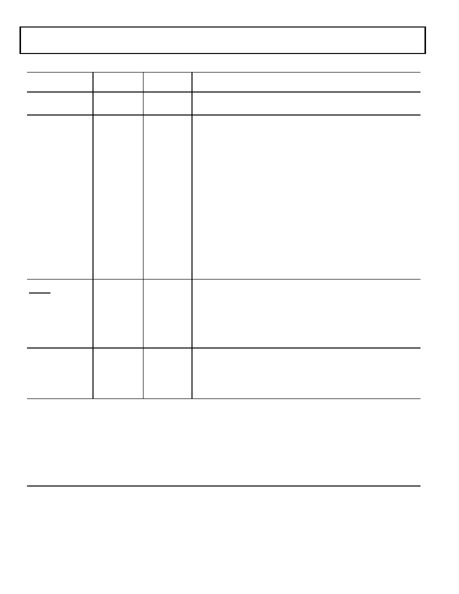
THD_P
I
Thermal Diode Anode. When not used, this pin can be left floating.
THD_M
O
Thermal Diode Cathode. When not used, this pin can be left floating.
MLBCLK
I
Media Local Bus Clock. This clock is generated by the MLB controller that is
synchronized to the MOST network and provides the timing for the entire MLB
interface at 49.152 MHz at FS = 48 kHz. When the MLB controller is not used, this
pin should be grounded.
MLBDAT
I/O/T in 3 pin
mode.
I in 5 pin mode.
High-Z
Media Local Bus Data. The MLBDAT line is driven by the transmitting MLB device
and is received by all other MLB devices including the MLB controller. The
MLBDAT line carries the actual data. In 5-pin MLB mode, this pin is an input only.
When the MLB controller is not used, this pin should be grounded.
MLBSIG
I/O/T in 3 pin
mode.
I in 5 pin mode
High-Z
Media Local Bus Signal. This is a multiplexed signal which carries the
Channel/Address generated by the MLB Controller, as well as the Command and
RxStatus bytes from MLB devices. In 5-pin mode, this pin is input only. When the
MLB controller is not used, this pin should be grounded.
MLBDO
O/T
High-Z
Media Local Bus Data Output (in 5 Pin Mode). This pin is used only in 5-pin MLB
mode and serves as the output data pin. When the MLB controller is not used, this
pin should be grounded.
MLBSO
O/T
High-Z
Media Local Bus Signal Output (in 5 Pin Mode). This pin is used only in 5-pin
MLB mode and serves as the output signal pin. When the MLB controller is not
used, this pin should be grounded.
SR_SCLK
I (ipu)
Shift Register Serial Clock. (Active high, rising edge sensitive)
SR_CLR
I (ipu)
Shift Register Reset. (Active low)
SR_SDI
I (ipu)
Shift Register Serial Data Input.
SR_SDO
O (ipu)
Driven Low
Shift Register Serial Data Output.
SR_LAT
I (ipu)
Shift Register Latch Clock Input. (Active high, rising edge sensitive)
SR_LDO17–0
O/T (ipu)
High-Z
Shift Register Parallel Data Output.
RTXI
I
RTC Crystal Input. If RTC is not used, then this pin needs to be NC (no connect)
and the RTC_PDN and RTC_BUSDIS bits of RTC_INIT register must be set to 1.
RTXO
O
RTC Crystal Output. If RTC is not used, then this pin needs to be NC (No Connect).
RTCLKOUT
O (ipd)
RTC Clock Output. For calibration purposes. The clock runs at 1 Hz. If RTC is not
used, then this pin needs to be NC (No Connect).
Table 11. Pin Descriptions (Continued)
Name
Type
State During/
After Reset
Description
The following symbols appear in the Type column of Table 11: A = asynchronous, I =input, O = output, S = synchronous, A/D = active drive,
O/D = open drain, and T = three-state, ipd = internal pull-down resistor, ipu = internal pull-up resistor.
The internal pull-up (ipu) and internal pull-down (ipd) resistors are designed to hold the internal path from the pins at the expected logic
levels. To pull-up or pull-down the external pads to the expected logic levels, use external resistors. Internal pull-up/pull-down resistors
cannot be enabled/disabled and the value of these resistors cannot be programmed. The range of an ipu resistor can be 26 kΩ to 63 kΩ. The
range of an ipd resistor can be 31 kΩ to 85 kΩ. The three-state voltage of ipu pads will not reach to full the VDD_EXT level; at typical conditions
the voltage is in the range of 2.3 V to 2.7 V.
In this table, all pins are LVTTL compliant with the exception of the thermal diode, shift register, and real-time clock (RTC) pins.
Not all pins are available in the 88-lead LFCSP_VQ and 100-lead LQFP package. For more information, see Table 2 on Page 3 and Table 62 on
Page 70.
相关PDF资料 |
PDF描述 |
|---|---|
| VI-24W-CY-F4 | CONVERTER MOD DC/DC 5.5V 50W |
| REC3-2412DR/H1M/SMD | CONV DC/DC 3W 24VIN +/-12VOUT |
| VE-J5F-IZ | CONVERTER MOD DC/DC 72V 25W |
| VI-24V-CY-F3 | CONVERTER MOD DC/DC 5.8V 50W |
| MAX6518UKP095+T | IC TEMP SENSOR SW SOT23-5 |
相关代理商/技术参数 |
参数描述 |
|---|---|
| ADSP-21478KCPZ-1A | 功能描述:IC DSP SHARK 200MHZ 88LFCSP RoHS:是 类别:集成电路 (IC) >> 嵌入式 - DSP(数字式信号处理器) 系列:SHARC® 标准包装:2 系列:StarCore 类型:SC140 内核 接口:DSI,以太网,RS-232 时钟速率:400MHz 非易失内存:外部 芯片上RAM:1.436MB 电压 - 输入/输出:3.30V 电压 - 核心:1.20V 工作温度:-40°C ~ 105°C 安装类型:表面贴装 封装/外壳:431-BFBGA,FCBGA 供应商设备封装:431-FCPBGA(20x20) 包装:托盘 |
| ADSP-21478KSWZ-1A | 功能描述:IC DSP SHARC 200MHZ LP 100LQFP RoHS:是 类别:集成电路 (IC) >> 嵌入式 - DSP(数字式信号处理器) 系列:SHARC® 标准包装:2 系列:StarCore 类型:SC140 内核 接口:DSI,以太网,RS-232 时钟速率:400MHz 非易失内存:外部 芯片上RAM:1.436MB 电压 - 输入/输出:3.30V 电压 - 核心:1.20V 工作温度:-40°C ~ 105°C 安装类型:表面贴装 封装/外壳:431-BFBGA,FCBGA 供应商设备封装:431-FCPBGA(20x20) 包装:托盘 |
| ADSP-21478KSWZ-2A | 功能描述:IC DSP SHARC 266MHZ LP 100LQFP RoHS:是 类别:集成电路 (IC) >> 嵌入式 - DSP(数字式信号处理器) 系列:SHARC® 标准包装:2 系列:StarCore 类型:SC140 内核 接口:DSI,以太网,RS-232 时钟速率:400MHz 非易失内存:外部 芯片上RAM:1.436MB 电压 - 输入/输出:3.30V 电压 - 核心:1.20V 工作温度:-40°C ~ 105°C 安装类型:表面贴装 封装/外壳:431-BFBGA,FCBGA 供应商设备封装:431-FCPBGA(20x20) 包装:托盘 |
| ADSP-21478KSWZ-ENG | 制造商:Analog Devices 功能描述:SHARC PROCESSOR - Trays |
| ADSP-21479 | 制造商:AD 制造商全称:Analog Devices 功能描述:SHARC Processor |
发布紧急采购,3分钟左右您将得到回复。