- 您现在的位置:买卖IC网 > PDF目录19388 > ADSP-2191MBSTZ-140 (Analog Devices Inc)IC DSP CONTROLLER 16BIT 144LQFP PDF资料下载
参数资料
| 型号: | ADSP-2191MBSTZ-140 |
| 厂商: | Analog Devices Inc |
| 文件页数: | 35/48页 |
| 文件大小: | 0K |
| 描述: | IC DSP CONTROLLER 16BIT 144LQFP |
| 标准包装: | 1 |
| 系列: | ADSP-21xx |
| 类型: | 定点 |
| 接口: | 主机接口,SPI,SSP,UART |
| 时钟速率: | 140MHz |
| 非易失内存: | 外部 |
| 芯片上RAM: | 160kB |
| 电压 - 输入/输出: | 3.00V,3.30V |
| 电压 - 核心: | 2.50V |
| 工作温度: | -40°C ~ 85°C |
| 安装类型: | 表面贴装 |
| 封装/外壳: | 144-LQFP |
| 供应商设备封装: | 144-LQFP(20x20) |
| 包装: | 托盘 |
| 其它名称: | ADSP-2191MBSTZ140 |
第1页第2页第3页第4页第5页第6页第7页第8页第9页第10页第11页第12页第13页第14页第15页第16页第17页第18页第19页第20页第21页第22页第23页第24页第25页第26页第27页第28页第29页第30页第31页第32页第33页第34页当前第35页第36页第37页第38页第39页第40页第41页第42页第43页第44页第45页第46页第47页第48页
ADSP-2191M
–40–
REV. A
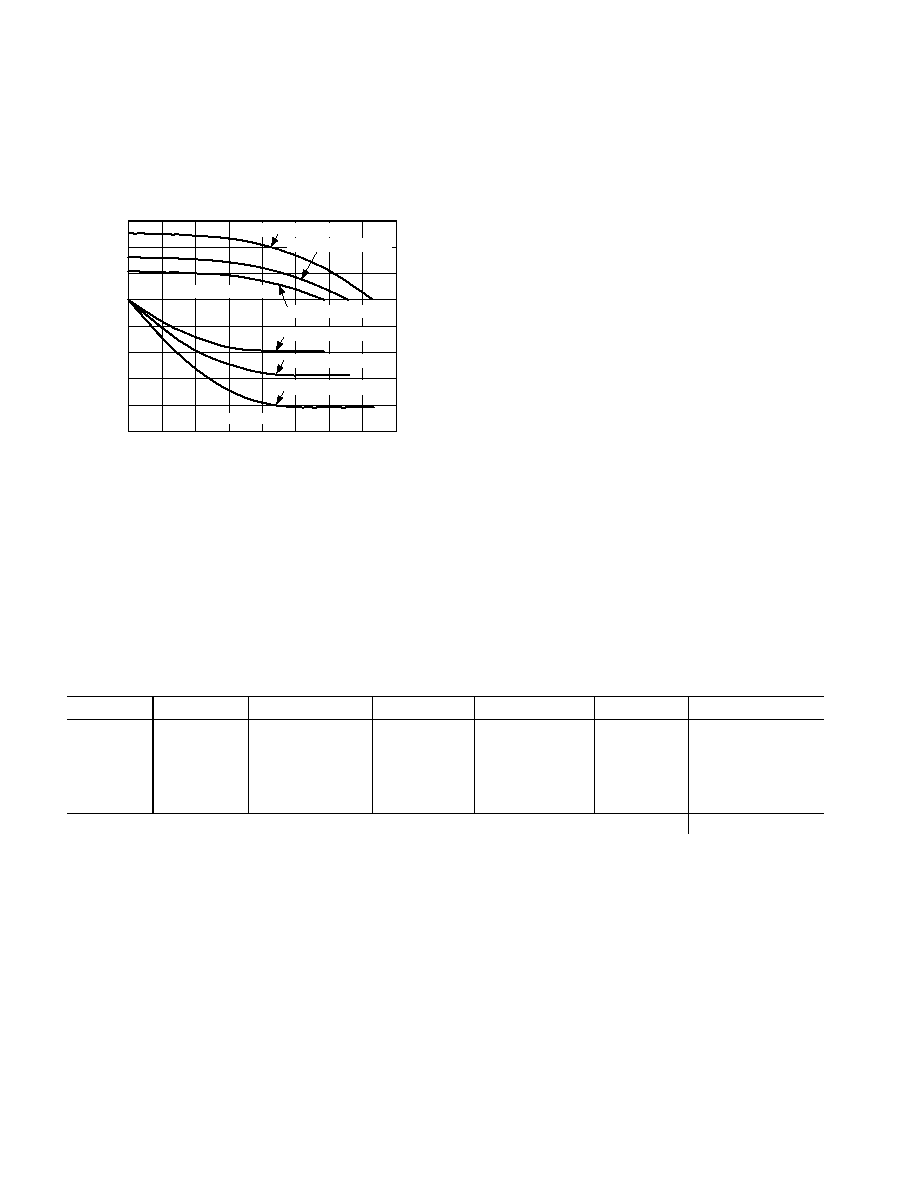
Output Drive Currents
Figure 25 shows typical I-V characteristics for the output drivers
of the ADSP-2191M. The curves represent the current drive
capability of the output drivers as a function of output voltage.
Power Dissipation
Total power dissipation has two components, one due to internal
circuitry and one due to the switching of external output drivers.
Internal power dissipation is dependent on the instruction
execution sequence and the data operands involved.
The external component of total power dissipation is caused by
the switching of output pins. Its magnitude depends on:
Number of output pins that switch during each cycle (O)
The maximum frequency at which they can switch (f)
Their load capacitance (C)
Their voltage swing (V
DD)
and is calculated by the formula below.
The load capacitance includes the processor’s package capaci-
tance (C
IN). The switching frequency includes driving the load
high and then back low. Address and data pins can drive high and
low at a maximum rate of 1/(2t
CK). The write strobe can switch
every cycle at a frequency of 1/t
CK. Select pins switch at 1/(2tCK),
but selects can switch on each cycle. For example, estimate P
EXT
with the following assumptions:
A system with one bank of external data memory—asyn-
chronous RAM (16-bit)
One 64K 16 RAM chip is used with a load of 10 pF
Maximum peripheral speed CCLK = 80 MHz, HCLK =
80 MHz
External data memory writes occur every other cycle, a
rate of 1/(4t
HCLK), with 50% of the pins switching
The bus cycle time is 80 MHz (t
HCLK = 12.5 ns)
The P
EXT equation is calculated for each class of pins that can
drive as shown in Table 23.
A typical power consumption can now be calculated for these
conditions by adding a typical internal power dissipation with the
following formula.
Where:
P
EXT is from Table 23
P
INT is IDDINT
2.5 V, using the calculation I
DDINT listed
Note that the conditions causing a worst-case P
EXT are different
from those causing a worst-case P
INT. Maximum PINT cannot
occur while 100% of the output pins are switching from all ones
to all zeros. Note also that it is not common for an application to
have 100% or even 50% of the outputs switching simultaneously.
Test Conditions
The DSP is tested for output enable, disable, and hold time.
Output Disable Time
Output pins are considered to be disabled when they stop driving,
go into a high impedance state, and start to decay from their
output high or low voltage. The time for the voltage on the bus
to decay by –V is dependent on the capacitive load, C
L and the
load current, I
L. This decay time can be approximated by the
equation below.
Figure 25. Typical Drive Currents
SOURCE (VDDEXT)VOLTAGE – V
03.5
0.5
1.0
1.5
2.0
2.5
3.0
S
O
U
R
C
E
(V
D
E
X
T
)
C
U
R
E
N
T
–
m
A
–100
–80
–60
–40
–20
0
20
40
60
4.0
VDDEXT =3.3V @ +25°C
VDDEXT =3.0V@ +85°C
VOH
VOL
VDDEXT =3.0V @ +85°C
VDDEXT =3.3V @ +25°C
VDDEXT =3.65V @ – 40°C
INPUT CURRENT
OUTPUT CURRENT
VDDEXT = 3.65V @ –40°C
P
EXT
OC
×
V
DD
2
×
f
×
=
Table 23. P
EXT Calculation Example
Pin Type
# of Pins
% Switching
C
f
VDD2
= PEXT
Address
15
50
10 pF
20 MHz
10.9 V
= 0.01635 W
MSx
10
10 pF
20 MHz
10.9 V
= 0.0 W
WR
1—
10 pF
40 MHz
10.9 V
= 0.00436 W
Data
16
50
10 pF
20 MHz
10.9 V
= 0.01744 W
CLKOUT
1
—
10 pF
80 MHz
10.9 V
= 0.00872 W
P
EXT = 0.04687 W
P
TOTAL
P
=
EXT
P
INT
+
相关PDF资料 |
PDF描述 |
|---|---|
| TLJA686M006R0500 | CAP TANT 68UF 6.3V 20% 1206 |
| MC7808CD2T | IC REG LDO 8V 1A D2PAK-3 |
| SWS600L-3 | POWER SUPPLY 3.3V 120A SGL OTPT |
| MC7808BT | IC REG LDO 8V 1A TO220AB |
| TLJA476M010R0600 | CAP TANT 47UF 10V 20% 1206 |
相关代理商/技术参数 |
参数描述 |
|---|---|
| ADSP-2191MKCA-160 | 功能描述:IC DSP CONTROLLER 16BIT 144MBGA RoHS:否 类别:集成电路 (IC) >> 嵌入式 - DSP(数字式信号处理器) 系列:ADSP-21xx 标准包装:2 系列:StarCore 类型:SC140 内核 接口:DSI,以太网,RS-232 时钟速率:400MHz 非易失内存:外部 芯片上RAM:1.436MB 电压 - 输入/输出:3.30V 电压 - 核心:1.20V 工作温度:-40°C ~ 105°C 安装类型:表面贴装 封装/外壳:431-BFBGA,FCBGA 供应商设备封装:431-FCPBGA(20x20) 包装:托盘 |
| ADSP-2191MKCAZ-160 | 功能描述:IC DSP CONTROLLER 16BIT 144MBGA RoHS:是 类别:集成电路 (IC) >> 嵌入式 - DSP(数字式信号处理器) 系列:ADSP-21xx 标准包装:40 系列:TMS320DM64x, DaVinci™ 类型:定点 接口:I²C,McASP,McBSP 时钟速率:400MHz 非易失内存:外部 芯片上RAM:160kB 电压 - 输入/输出:3.30V 电压 - 核心:1.20V 工作温度:0°C ~ 90°C 安装类型:表面贴装 封装/外壳:548-BBGA,FCBGA 供应商设备封装:548-FCBGA(27x27) 包装:托盘 配用:TMDSDMK642-0E-ND - DEVELPER KIT W/NTSC CAMERA296-23038-ND - DSP STARTER KIT FOR TMS320C6416296-23059-ND - FLASHBURN PORTING KIT296-23058-ND - EVAL MODULE FOR DM642TMDSDMK642-ND - DEVELOPER KIT W/NTSC CAMERA |
| ADSP-2191MKST-160 | 制造商:Analog Devices 功能描述:DSP 16-Bit 160MHz 160MIPS 144-Pin LQFP 制造商:Analog Devices 功能描述:Digital Signal Processor IC Supply Volta |
| ADSP-2191MKSTZ-160 | 功能描述:IC DSP CONTROLLER 16BIT 144LQFP RoHS:是 类别:集成电路 (IC) >> 嵌入式 - DSP(数字式信号处理器) 系列:ADSP-21xx 标准包装:40 系列:TMS320DM64x, DaVinci™ 类型:定点 接口:I²C,McASP,McBSP 时钟速率:400MHz 非易失内存:外部 芯片上RAM:160kB 电压 - 输入/输出:3.30V 电压 - 核心:1.20V 工作温度:0°C ~ 90°C 安装类型:表面贴装 封装/外壳:548-BBGA,FCBGA 供应商设备封装:548-FCBGA(27x27) 包装:托盘 配用:TMDSDMK642-0E-ND - DEVELPER KIT W/NTSC CAMERA296-23038-ND - DSP STARTER KIT FOR TMS320C6416296-23059-ND - FLASHBURN PORTING KIT296-23058-ND - EVAL MODULE FOR DM642TMDSDMK642-ND - DEVELOPER KIT W/NTSC CAMERA |
| ADSP-2195MBCA-140 | 制造商:Analog Devices 功能描述:DSP Fixed-Point 24-Bit 140MHz 140MIPS 144-Pin CSP-BGA 制造商:Rochester Electronics LLC 功能描述:16-BIT,140 MIPS, 2.5V, 80KBYTES RAM - Bulk |
发布紧急采购,3分钟左右您将得到回复。