- 您现在的位置:买卖IC网 > PDF目录19388 > ADSP-2191MBSTZ-140 (Analog Devices Inc)IC DSP CONTROLLER 16BIT 144LQFP PDF资料下载
参数资料
| 型号: | ADSP-2191MBSTZ-140 |
| 厂商: | Analog Devices Inc |
| 文件页数: | 36/48页 |
| 文件大小: | 0K |
| 描述: | IC DSP CONTROLLER 16BIT 144LQFP |
| 标准包装: | 1 |
| 系列: | ADSP-21xx |
| 类型: | 定点 |
| 接口: | 主机接口,SPI,SSP,UART |
| 时钟速率: | 140MHz |
| 非易失内存: | 外部 |
| 芯片上RAM: | 160kB |
| 电压 - 输入/输出: | 3.00V,3.30V |
| 电压 - 核心: | 2.50V |
| 工作温度: | -40°C ~ 85°C |
| 安装类型: | 表面贴装 |
| 封装/外壳: | 144-LQFP |
| 供应商设备封装: | 144-LQFP(20x20) |
| 包装: | 托盘 |
| 其它名称: | ADSP-2191MBSTZ140 |
第1页第2页第3页第4页第5页第6页第7页第8页第9页第10页第11页第12页第13页第14页第15页第16页第17页第18页第19页第20页第21页第22页第23页第24页第25页第26页第27页第28页第29页第30页第31页第32页第33页第34页第35页当前第36页第37页第38页第39页第40页第41页第42页第43页第44页第45页第46页第47页第48页
–41–
REV. A
ADSP-2191M
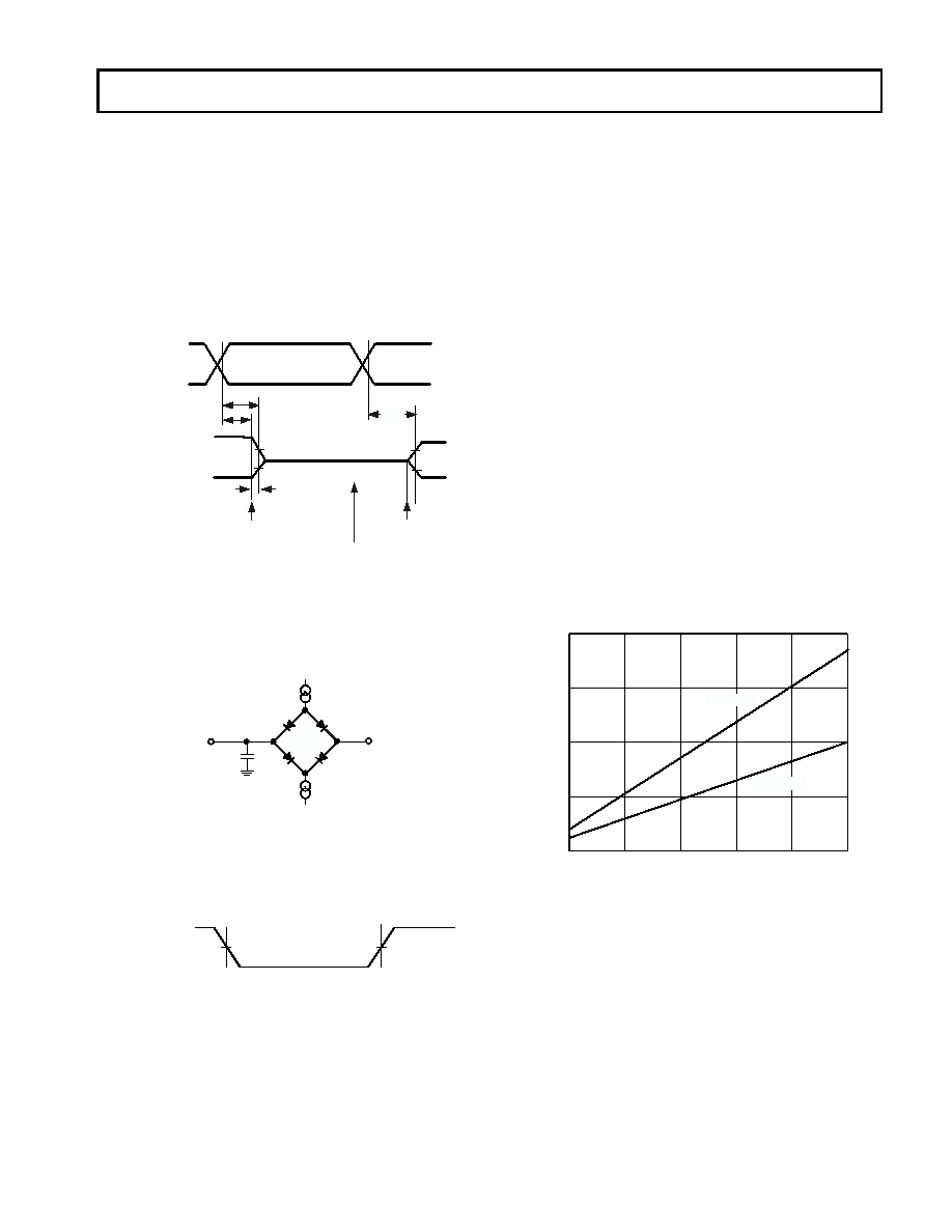
The output disable time t
DIS is the difference between tMEASURED
and t
interval from when the reference signal switches to when the
output voltage decays –V from the measured output high or
output low voltage. The t
DECAY is calculated with test loads CL
and I
L, and with – V equal to 0.5 V.
Output Enable Time
Output pins are considered to be enabled when they have made
a transition from a high impedance state to when they start
driving. The output enable time t
ENA is the interval from when a
reference signal reaches a high or low voltage level to when the
output has reached a specified high or low trip point, as shown
in the Output Enable/Disable diagram (Figure 26). If multiple
pins (such as the data bus) are enabled, the measurement value
is that of the first pin to start driving.
Example System Hold Time Calculation
To determine the data output hold time in a particular system,
first calculate t
DECAY using the equation at Output Disable Time
on Page 40. Choose –V to be the difference between the
ADSP-2191M’s output voltage and the input threshold for the
device requiring the hold time. A typical –V will be 0.4 V. C
L is
the total bus capacitance (per data line), and I
L is the total leakage
or three-state current (per data line). The hold time will be t
DECAY
plus the minimum disable time (i.e., t
DATRWH for the
write cycle).
Capacitive Loading
Output delays and holds are based on standard capacitive loads:
50 pF on all pins (see Figure 30). The delay and hold specifica-
tions given should be derated by a factor of 1.5 ns/50 pF for loads
show how output rise time varies with capacitance. These figures
also show graphically how output delays and holds vary with load
capacitance. (Note that this graph or derating does not apply to
output disable delays; see Output Disable Time on Page 40.) The
graphs in these figures may not be linear outside the ranges
shown.
Environmental Conditions
The thermal characteristics in which the DSP is operating
influence performance.
Thermal Characteristics
The ADSP-2191M comes in a 144-lead LQFP or 144-lead Ball
Grid Array (mini-BGA) package. The ADSP-2191M is specified
for an ambient temperature (T
AMB) as calculated using the
formula below.
Figure 26. Output Enable/Disable
Figure 27. Equivalent Device Loading for AC
Measurements (Includes All Fixtures)
Figure 28. Voltage Reference Levels for AC
Measurements (Except Output Enable/Disable)
t
DECAY
C
L V
I
L
---------------
=
REFERENCE
SIGNAL
tDIS
OUTPUT STARTS
DRIVING
VOH (MEASURED) – V2.0V
VOL (MEASURED) + V1.0V
tMEASURED
VOH (MEASURED)
VOL (MEASURED)
HIGH IMPEDANCE STATE.
TEST CONDITIONS CAUSE THIS VOLTAGE
TO BE APPROXIMATELY 1.5V
OUTPUT STOPS
DRIVING
tDECAY
tENA
1.5V
50pF
TO
OUTPUT
PIN
IOL
IOH
INPUT
OR
OUTPUT
1.5V
Figure 29. Typical Output Rise Time (10%-90%,
VDDEXT = Minimum at Maximum Ambient Operating
Temperature) vs. Load Capacitance
40
0
30
20
10
LOAD CAPACITANCE – pF
0250
50
100
150
200
R
IS
E
A
N
D
F
A
L
T
IM
E
S
–
n
s
(1
0
%
–
9
0
%
)
FALL TIME
RISE TIME
相关PDF资料 |
PDF描述 |
|---|---|
| TLJA686M006R0500 | CAP TANT 68UF 6.3V 20% 1206 |
| MC7808CD2T | IC REG LDO 8V 1A D2PAK-3 |
| SWS600L-3 | POWER SUPPLY 3.3V 120A SGL OTPT |
| MC7808BT | IC REG LDO 8V 1A TO220AB |
| TLJA476M010R0600 | CAP TANT 47UF 10V 20% 1206 |
相关代理商/技术参数 |
参数描述 |
|---|---|
| ADSP-2191MKCA-160 | 功能描述:IC DSP CONTROLLER 16BIT 144MBGA RoHS:否 类别:集成电路 (IC) >> 嵌入式 - DSP(数字式信号处理器) 系列:ADSP-21xx 标准包装:2 系列:StarCore 类型:SC140 内核 接口:DSI,以太网,RS-232 时钟速率:400MHz 非易失内存:外部 芯片上RAM:1.436MB 电压 - 输入/输出:3.30V 电压 - 核心:1.20V 工作温度:-40°C ~ 105°C 安装类型:表面贴装 封装/外壳:431-BFBGA,FCBGA 供应商设备封装:431-FCPBGA(20x20) 包装:托盘 |
| ADSP-2191MKCAZ-160 | 功能描述:IC DSP CONTROLLER 16BIT 144MBGA RoHS:是 类别:集成电路 (IC) >> 嵌入式 - DSP(数字式信号处理器) 系列:ADSP-21xx 标准包装:40 系列:TMS320DM64x, DaVinci™ 类型:定点 接口:I²C,McASP,McBSP 时钟速率:400MHz 非易失内存:外部 芯片上RAM:160kB 电压 - 输入/输出:3.30V 电压 - 核心:1.20V 工作温度:0°C ~ 90°C 安装类型:表面贴装 封装/外壳:548-BBGA,FCBGA 供应商设备封装:548-FCBGA(27x27) 包装:托盘 配用:TMDSDMK642-0E-ND - DEVELPER KIT W/NTSC CAMERA296-23038-ND - DSP STARTER KIT FOR TMS320C6416296-23059-ND - FLASHBURN PORTING KIT296-23058-ND - EVAL MODULE FOR DM642TMDSDMK642-ND - DEVELOPER KIT W/NTSC CAMERA |
| ADSP-2191MKST-160 | 制造商:Analog Devices 功能描述:DSP 16-Bit 160MHz 160MIPS 144-Pin LQFP 制造商:Analog Devices 功能描述:Digital Signal Processor IC Supply Volta |
| ADSP-2191MKSTZ-160 | 功能描述:IC DSP CONTROLLER 16BIT 144LQFP RoHS:是 类别:集成电路 (IC) >> 嵌入式 - DSP(数字式信号处理器) 系列:ADSP-21xx 标准包装:40 系列:TMS320DM64x, DaVinci™ 类型:定点 接口:I²C,McASP,McBSP 时钟速率:400MHz 非易失内存:外部 芯片上RAM:160kB 电压 - 输入/输出:3.30V 电压 - 核心:1.20V 工作温度:0°C ~ 90°C 安装类型:表面贴装 封装/外壳:548-BBGA,FCBGA 供应商设备封装:548-FCBGA(27x27) 包装:托盘 配用:TMDSDMK642-0E-ND - DEVELPER KIT W/NTSC CAMERA296-23038-ND - DSP STARTER KIT FOR TMS320C6416296-23059-ND - FLASHBURN PORTING KIT296-23058-ND - EVAL MODULE FOR DM642TMDSDMK642-ND - DEVELOPER KIT W/NTSC CAMERA |
| ADSP-2195MBCA-140 | 制造商:Analog Devices 功能描述:DSP Fixed-Point 24-Bit 140MHz 140MIPS 144-Pin CSP-BGA 制造商:Rochester Electronics LLC 功能描述:16-BIT,140 MIPS, 2.5V, 80KBYTES RAM - Bulk |
发布紧急采购,3分钟左右您将得到回复。