- 您现在的位置:买卖IC网 > PDF目录19403 > ADSP-BF504KCPZ-3F (Analog Devices Inc)IC CCD SIGNAL PROCESSOR 88LFCSP PDF资料下载
参数资料
| 型号: | ADSP-BF504KCPZ-3F |
| 厂商: | Analog Devices Inc |
| 文件页数: | 45/80页 |
| 文件大小: | 0K |
| 描述: | IC CCD SIGNAL PROCESSOR 88LFCSP |
| 视频文件: | Blackfin? BF50x Processor Family |
| 标准包装: | 1 |
| 系列: | Blackfin® |
| 类型: | 定点 |
| 接口: | CAN,EBI/EMI,I²C,IrDA,PPI,SPI,SPORT,UART/USART |
| 时钟速率: | 300MHz |
| 非易失内存: | 闪存(16MB) |
| 芯片上RAM: | 68kB |
| 电压 - 输入/输出: | 3.30V |
| 电压 - 核心: | 1.31V |
| 工作温度: | 0°C ~ 70°C |
| 安装类型: | 表面贴装 |
| 封装/外壳: | 88-VFQFN 裸露焊盘,CSP |
| 供应商设备封装: | 88-LFCSP(12x12) |
| 包装: | 托盘 |
第1页第2页第3页第4页第5页第6页第7页第8页第9页第10页第11页第12页第13页第14页第15页第16页第17页第18页第19页第20页第21页第22页第23页第24页第25页第26页第27页第28页第29页第30页第31页第32页第33页第34页第35页第36页第37页第38页第39页第40页第41页第42页第43页第44页当前第45页第46页第47页第48页第49页第50页第51页第52页第53页第54页第55页第56页第57页第58页第59页第60页第61页第62页第63页第64页第65页第66页第67页第68页第69页第70页第71页第72页第73页第74页第75页第76页第77页第78页第79页第80页
Rev. A
|
Page 5 of 80
|
July 2011
ADSP-BF504/ADSP-BF504F/ADSP-BF506F
Blackfin processors support a modified Harvard architecture in
combination with a hierarchical memory structure. Level 1 (L1)
memories are those that typically operate at the full processor
speed with little or no latency. At the L1 level, the instruction
memory holds instructions only. The data memory holds data,
and a dedicated scratchpad data memory stores stack and local
variable information.
In addition, multiple L1 memory blocks are provided, offering a
configurable mix of SRAM and cache. The memory manage-
ment unit (MMU) provides memory protection for individual
tasks that may be operating on the core and can protect system
registers from unintended access.
The architecture provides three modes of operation: user mode,
supervisor mode, and emulation mode. User mode has
restricted access to certain system resources, thus providing a
protected software environment, while supervisor mode has
unrestricted access to the system and core resources.
The Blackfin processor instruction set has been optimized so
that 16-bit opcodes represent the most frequently used instruc-
tions, resulting in excellent compiled code density. Complex
DSP instructions are encoded into 32-bit opcodes, representing
fully featured multifunction instructions. Blackfin processors
support a limited multi-issue capability, where a 32-bit instruc-
tion can be issued in parallel with two 16-bit instructions,
allowing the programmer to use many of the core resources in a
single instruction cycle.
The Blackfin processor assembly language uses an algebraic syn-
tax for ease of coding and readability. The architecture has been
optimized for use in conjunction with the C/C++ compiler,
resulting in fast and efficient software implementations.
MEMORY ARCHITECTURE
The Blackfin processor views memory as a single unified
4G byte address space, using 32-bit addresses. All resources,
including internal memory, external memory, and I/O control
registers, occupy separate sections of this common address
space. The memory portions of this address space are arranged
in a hierarchical structure to provide a good cost/performance
balance of some very fast, low latency core-accessible memory
as cache or SRAM and to provide larger, lower cost and perfor-
mance interface-accessible memory systems. See Figure 3.
The core-accessible L1 memory system is the highest perfor-
mance memory available to the Blackfin processor. The
interface-accessible memory system, accessed through the
external bus interface unit (EBIU), provides access to the inter-
nal flash memory and boot ROM.
The memory DMA controller provides high bandwidth data
movement capability. It can perform block transfers of code
or data between the internal memory and the external
memory spaces.
Internal (Core-Accessible) Memory
The processor has three blocks of core-accessible memory,
providing high-bandwidth access to the core.
The first block is the L1 instruction memory, consisting of
32K bytes SRAM, of which 16K bytes can be configured as a
four-way set-associative cache. This memory is accessed at full
processor speed.
The second core-accessible memory block is the L1 data mem-
ory, consisting of 32K bytes of SRAM, of which 16K bytes may
be configured as cache. This memory block is accessed at full
processor speed.
The third memory block is 4K bytes of scratchpad SRAM, which
runs at the same speed as the L1 memories, but this memory is
only accessible as data SRAM and cannot be configured as cache
memory.
External (Interface-Accessible) Memory
External memory is accessed via the EBIU memory port. This
16-bit interface provides a glueless connection to the internal
flash memory and boot ROM. Internal flash memory ships from
the factory in an erased state except for Block 0 of the parameter
bank. Block 0 of the Flash memory parameter bank ships from
the factory in an unknown state. An erase operation should be
performed prior to programming this block.
I/O Memory Space
The processor does not define a separate I/O space. All
resources are mapped through the flat 32-bit address space.
On-chip I/O devices have their control registers mapped into
memory-mapped registers (MMRs) at addresses near the top of
the 4G byte address space. These are separated into two smaller
blocks. One contains the control MMRs for all core functions,
and the other contains the registers needed for setup and con-
trol of the on-chip peripherals outside of the core. The MMRs
are accessible only in supervisor and emulation modes and
appear as reserved space to on-chip peripherals.
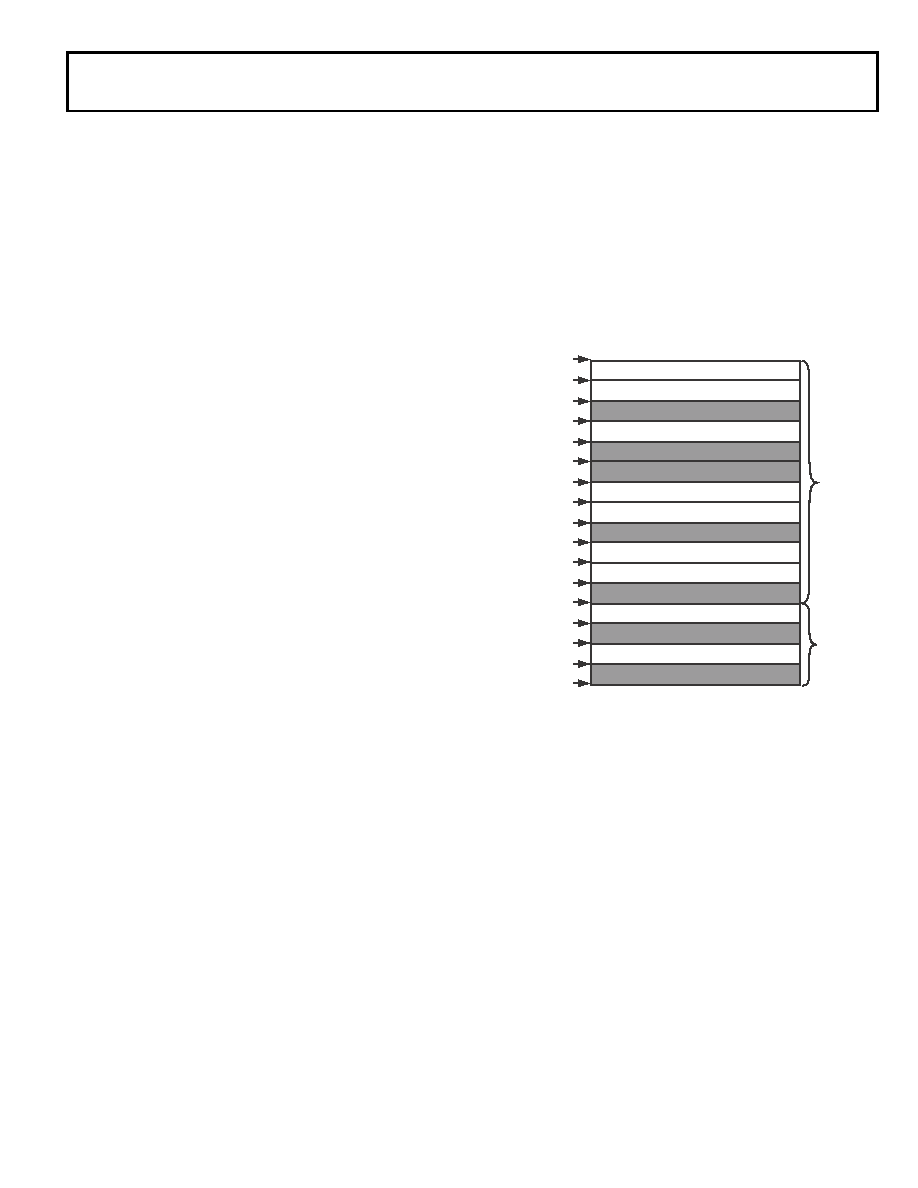
Figure 3. Internal/External Memory Map
INTERNAL
(CORE-A
CCESSIBLE)
MEMOR
Y
MAP
EXTERNAL
(INTERF
A
CE-A
CCESSIBLE)
MEMOR
Y
MAP
0x0000 0000
0x2000 0000
0x2040 0000
0xEF00 0000
0xEF00 1000
0xFF80 0000
0xFF80 4000
0xFF80 8000
0xFFA0 0000
0xFFA0 4000
0xFFA0 8000
0xFFA1 4000
0xFFB0 0000
0xFFB0 1000
0xFFC0 0000
0xFFE0 0000
0xFFFF FFFF
SYNC FLASH (32M BITS) *
RESERVED
BOOT ROM (4K BYTES)
L1 DATA BANK A SRAM (16K BYTES)
RESERVED
L1 DATA BANK A SRAM/CACHE (16K BYTES)
RESERVED
L1 INSTRUCTION SRAM/CACHE (16K BYTES)
RESERVED
L1 INSTRUCTION BANK A SRAM (16K BYTES)
RESERVED
INTERNAL SCRATCHPAD RAM (4K BYTES)
RESERVED
SYSTEM MEMORY MAPPED REGISTERS
CORE MEMORY MAPPED REGISTERS
* AVAILABLE ON PARTS WITH SYNC FLASH (F)
相关PDF资料 |
PDF描述 |
|---|---|
| ADSP-BF536BBCZ3BRL | IC DSP CTLR 16BIT 208BGA |
| ZWS240PAF36 | PWR SUP 36V 241.2W 6.7A |
| ZWS240PAF48 | PWR SUP 48V 240W 5A |
| MAX6501UKP125+T | IC TEMP SWITCH SOT23-5 |
| ZWQ1305223 | PWRSUP QUAD 5V/+12V/-12V/3.3V |
相关代理商/技术参数 |
参数描述 |
|---|---|
| ADSP-BF504KCPZ-4 | 功能描述:IC CCD SIGNAL PROCESSOR 88LFCSP RoHS:是 类别:集成电路 (IC) >> 嵌入式 - DSP(数字式信号处理器) 系列:Blackfin® 标准包装:2 系列:StarCore 类型:SC140 内核 接口:DSI,以太网,RS-232 时钟速率:400MHz 非易失内存:外部 芯片上RAM:1.436MB 电压 - 输入/输出:3.30V 电压 - 核心:1.20V 工作温度:-40°C ~ 105°C 安装类型:表面贴装 封装/外壳:431-BFBGA,FCBGA 供应商设备封装:431-FCPBGA(20x20) 包装:托盘 |
| ADSP-BF504KCPZ-4F | 功能描述:IC CCD SIGNAL PROCESSOR 88LFCSP RoHS:是 类别:集成电路 (IC) >> 嵌入式 - DSP(数字式信号处理器) 系列:Blackfin® 标准包装:2 系列:StarCore 类型:SC140 内核 接口:DSI,以太网,RS-232 时钟速率:400MHz 非易失内存:外部 芯片上RAM:1.436MB 电压 - 输入/输出:3.30V 电压 - 核心:1.20V 工作温度:-40°C ~ 105°C 安装类型:表面贴装 封装/外壳:431-BFBGA,FCBGA 供应商设备封装:431-FCPBGA(20x20) 包装:托盘 |
| ADSP-BF506BSWZ-3F | 功能描述:IC DSP 400MHZ 1.4V 120LQFP RoHS:是 类别:集成电路 (IC) >> 嵌入式 - DSP(数字式信号处理器) 系列:Blackfin® 标准包装:40 系列:TMS320DM64x, DaVinci™ 类型:定点 接口:I²C,McASP,McBSP 时钟速率:400MHz 非易失内存:外部 芯片上RAM:160kB 电压 - 输入/输出:3.30V 电压 - 核心:1.20V 工作温度:0°C ~ 90°C 安装类型:表面贴装 封装/外壳:548-BBGA,FCBGA 供应商设备封装:548-FCBGA(27x27) 包装:托盘 配用:TMDSDMK642-0E-ND - DEVELPER KIT W/NTSC CAMERA296-23038-ND - DSP STARTER KIT FOR TMS320C6416296-23059-ND - FLASHBURN PORTING KIT296-23058-ND - EVAL MODULE FOR DM642TMDSDMK642-ND - DEVELOPER KIT W/NTSC CAMERA |
| ADSP-BF506BSWZ-4F | 功能描述:IC DSP 400MHZ 1.4V 120LQFP RoHS:是 类别:集成电路 (IC) >> 嵌入式 - DSP(数字式信号处理器) 系列:Blackfin® 标准包装:40 系列:TMS320DM64x, DaVinci™ 类型:定点 接口:I²C,McASP,McBSP 时钟速率:400MHz 非易失内存:外部 芯片上RAM:160kB 电压 - 输入/输出:3.30V 电压 - 核心:1.20V 工作温度:0°C ~ 90°C 安装类型:表面贴装 封装/外壳:548-BBGA,FCBGA 供应商设备封装:548-FCBGA(27x27) 包装:托盘 配用:TMDSDMK642-0E-ND - DEVELPER KIT W/NTSC CAMERA296-23038-ND - DSP STARTER KIT FOR TMS320C6416296-23059-ND - FLASHBURN PORTING KIT296-23058-ND - EVAL MODULE FOR DM642TMDSDMK642-ND - DEVELOPER KIT W/NTSC CAMERA |
| ADSP-BF506BSWZ-4FX | 制造商:Analog Devices 功能描述:- Trays |
发布紧急采购,3分钟左右您将得到回复。