- 您现在的位置:买卖IC网 > PDF目录19403 > ADSP-BF504KCPZ-3F (Analog Devices Inc)IC CCD SIGNAL PROCESSOR 88LFCSP PDF资料下载
参数资料
| 型号: | ADSP-BF504KCPZ-3F |
| 厂商: | Analog Devices Inc |
| 文件页数: | 65/80页 |
| 文件大小: | 0K |
| 描述: | IC CCD SIGNAL PROCESSOR 88LFCSP |
| 视频文件: | Blackfin? BF50x Processor Family |
| 标准包装: | 1 |
| 系列: | Blackfin® |
| 类型: | 定点 |
| 接口: | CAN,EBI/EMI,I²C,IrDA,PPI,SPI,SPORT,UART/USART |
| 时钟速率: | 300MHz |
| 非易失内存: | 闪存(16MB) |
| 芯片上RAM: | 68kB |
| 电压 - 输入/输出: | 3.30V |
| 电压 - 核心: | 1.31V |
| 工作温度: | 0°C ~ 70°C |
| 安装类型: | 表面贴装 |
| 封装/外壳: | 88-VFQFN 裸露焊盘,CSP |
| 供应商设备封装: | 88-LFCSP(12x12) |
| 包装: | 托盘 |
第1页第2页第3页第4页第5页第6页第7页第8页第9页第10页第11页第12页第13页第14页第15页第16页第17页第18页第19页第20页第21页第22页第23页第24页第25页第26页第27页第28页第29页第30页第31页第32页第33页第34页第35页第36页第37页第38页第39页第40页第41页第42页第43页第44页第45页第46页第47页第48页第49页第50页第51页第52页第53页第54页第55页第56页第57页第58页第59页第60页第61页第62页第63页第64页当前第65页第66页第67页第68页第69页第70页第71页第72页第73页第74页第75页第76页第77页第78页第79页第80页
Rev. A
|
Page 68 of 80
|
July 2011
ADSP-BF504/ADSP-BF504F/ADSP-BF506F
down for a relatively long duration between these bursts of sev-
eral conversions. When the ADC is in partial power-down, all
analog circuitry is powered down except for the on-chip refer-
ence and reference buffer.
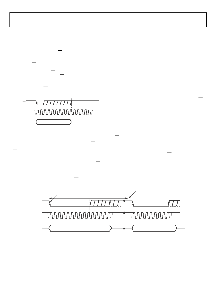
To enter partial power-down mode, the conversion process
must be interrupted by bringing CS high anywhere after the sec-
ond falling edge of ADSCLK and before the 10th falling edge of
ADSCLK, as shown in Figure 81 (Entering Partial Power-Down
Mode). Once CS is brought high in this window of ADSCLKs,
the part enters partial power-down, the conversion that was ini-
tiated by the falling edge of CS is terminated, and DOUTA and
DOUTB go back into three-state. If CS is brought high before the
second ADSCLK falling edge, the part remains in normal mode
and does not power down. This avoids accidental power-down
due to glitches on the CS line.
To exit this mode of operation and power up the ADC again, a
dummy conversion is performed. On the falling edge of CS, the
device begins to power up and continues to power up as long as
CS is held low until after the falling edge of the 10th ADSCLK.
The device is fully powered up after approximately 1 μs has
elapsed, and valid data results from the next conversion, as
shown in Figure 82 (Exiting Partial Power-Down Mode). If CS
is brought high before the second falling edge of ADSCLK, the
ADC again goes into partial power-down. This avoids acciden-
tal power-up due to glitches on the CS line. Although the device
may begin to power up on the falling edge of CS, it powers down
again on the rising edge of CS. If the ADC is already in partial
power-down mode and CS is brought high between the second
and 10th falling edges of ADSCLK, the device enters full power-
down mode.
Full Power-Down Mode
This mode is intended for use in applications where throughput
rates slower than those in the partial power-down mode are
required, as power-up from a full power-down takes substan-
tially longer than that from partial power-down. This mode is
more suited to applications where a series of conversions per-
formed at a relatively high throughput rate are followed by a
long period of inactivity and thus power-down. When the ADC
is in full power-down, all analog circuitry is powered down. Full
power-down is entered in a similar way as partial power-down,
except the timing sequence shown in Figure 81 (Entering Partial
Power-Down Mode) must be executed twice. The conversion
process must be interrupted in a similar fashion by bringing CS
high anywhere after the second falling edge of ADSCLK and
before the 10th falling edge of ADSCLK. The device enters par-
tial power-down at this point. To reach full power-down, the
next conversion cycle must be interrupted in the same way, as
shown in Figure 83 (Entering Full Power-Down Mode). Once
CS is brought high in this window of ADSCLKs, the part com-
pletely powers down.
Note that it is not necessary to complete the 14 ADSCLKs once
CS is brought high to enter a power-down mode.
To exit full power-down and power up the ADC, a dummy con-
version is performed, as when powering up from partial power-
down. On the falling edge of CS, the device begins to power up
and continues to power up, as long as CS is held low until after
the falling edge of the 10th ADSCLK. The required power-up
time must elapse before a conversion can be initiated, as shown
in Figure 84 (Exiting Full Power-Down Mode). See the Power-
Up Times section for the power-up times associated with the
ADC.
Figure 81. Entering Partial Power-Down Mode
ADSCLK
THREE-STATE
CS
DOUTA
DOUTB
114
10
2
Figure 82. Exiting Partial Power-Down Mode
ADSCLK
CS
DOUTA
DOUTB
INVALID DATA
VALID DATA
110
14
1
THE PART BEGINS
TO POWER UP.
THE PART IS FULLY
POWERED UP; SEE
POWER-UP TIMES
SECTION.
tPOWER-UP1
相关PDF资料 |
PDF描述 |
|---|---|
| ADSP-BF536BBCZ3BRL | IC DSP CTLR 16BIT 208BGA |
| ZWS240PAF36 | PWR SUP 36V 241.2W 6.7A |
| ZWS240PAF48 | PWR SUP 48V 240W 5A |
| MAX6501UKP125+T | IC TEMP SWITCH SOT23-5 |
| ZWQ1305223 | PWRSUP QUAD 5V/+12V/-12V/3.3V |
相关代理商/技术参数 |
参数描述 |
|---|---|
| ADSP-BF504KCPZ-4 | 功能描述:IC CCD SIGNAL PROCESSOR 88LFCSP RoHS:是 类别:集成电路 (IC) >> 嵌入式 - DSP(数字式信号处理器) 系列:Blackfin® 标准包装:2 系列:StarCore 类型:SC140 内核 接口:DSI,以太网,RS-232 时钟速率:400MHz 非易失内存:外部 芯片上RAM:1.436MB 电压 - 输入/输出:3.30V 电压 - 核心:1.20V 工作温度:-40°C ~ 105°C 安装类型:表面贴装 封装/外壳:431-BFBGA,FCBGA 供应商设备封装:431-FCPBGA(20x20) 包装:托盘 |
| ADSP-BF504KCPZ-4F | 功能描述:IC CCD SIGNAL PROCESSOR 88LFCSP RoHS:是 类别:集成电路 (IC) >> 嵌入式 - DSP(数字式信号处理器) 系列:Blackfin® 标准包装:2 系列:StarCore 类型:SC140 内核 接口:DSI,以太网,RS-232 时钟速率:400MHz 非易失内存:外部 芯片上RAM:1.436MB 电压 - 输入/输出:3.30V 电压 - 核心:1.20V 工作温度:-40°C ~ 105°C 安装类型:表面贴装 封装/外壳:431-BFBGA,FCBGA 供应商设备封装:431-FCPBGA(20x20) 包装:托盘 |
| ADSP-BF506BSWZ-3F | 功能描述:IC DSP 400MHZ 1.4V 120LQFP RoHS:是 类别:集成电路 (IC) >> 嵌入式 - DSP(数字式信号处理器) 系列:Blackfin® 标准包装:40 系列:TMS320DM64x, DaVinci™ 类型:定点 接口:I²C,McASP,McBSP 时钟速率:400MHz 非易失内存:外部 芯片上RAM:160kB 电压 - 输入/输出:3.30V 电压 - 核心:1.20V 工作温度:0°C ~ 90°C 安装类型:表面贴装 封装/外壳:548-BBGA,FCBGA 供应商设备封装:548-FCBGA(27x27) 包装:托盘 配用:TMDSDMK642-0E-ND - DEVELPER KIT W/NTSC CAMERA296-23038-ND - DSP STARTER KIT FOR TMS320C6416296-23059-ND - FLASHBURN PORTING KIT296-23058-ND - EVAL MODULE FOR DM642TMDSDMK642-ND - DEVELOPER KIT W/NTSC CAMERA |
| ADSP-BF506BSWZ-4F | 功能描述:IC DSP 400MHZ 1.4V 120LQFP RoHS:是 类别:集成电路 (IC) >> 嵌入式 - DSP(数字式信号处理器) 系列:Blackfin® 标准包装:40 系列:TMS320DM64x, DaVinci™ 类型:定点 接口:I²C,McASP,McBSP 时钟速率:400MHz 非易失内存:外部 芯片上RAM:160kB 电压 - 输入/输出:3.30V 电压 - 核心:1.20V 工作温度:0°C ~ 90°C 安装类型:表面贴装 封装/外壳:548-BBGA,FCBGA 供应商设备封装:548-FCBGA(27x27) 包装:托盘 配用:TMDSDMK642-0E-ND - DEVELPER KIT W/NTSC CAMERA296-23038-ND - DSP STARTER KIT FOR TMS320C6416296-23059-ND - FLASHBURN PORTING KIT296-23058-ND - EVAL MODULE FOR DM642TMDSDMK642-ND - DEVELOPER KIT W/NTSC CAMERA |
| ADSP-BF506BSWZ-4FX | 制造商:Analog Devices 功能描述:- Trays |
发布紧急采购,3分钟左右您将得到回复。