- 您现在的位置:买卖IC网 > PDF目录19403 > ADSP-BF504KCPZ-3F (Analog Devices Inc)IC CCD SIGNAL PROCESSOR 88LFCSP PDF资料下载
参数资料
| 型号: | ADSP-BF504KCPZ-3F |
| 厂商: | Analog Devices Inc |
| 文件页数: | 6/80页 |
| 文件大小: | 0K |
| 描述: | IC CCD SIGNAL PROCESSOR 88LFCSP |
| 视频文件: | Blackfin? BF50x Processor Family |
| 标准包装: | 1 |
| 系列: | Blackfin® |
| 类型: | 定点 |
| 接口: | CAN,EBI/EMI,I²C,IrDA,PPI,SPI,SPORT,UART/USART |
| 时钟速率: | 300MHz |
| 非易失内存: | 闪存(16MB) |
| 芯片上RAM: | 68kB |
| 电压 - 输入/输出: | 3.30V |
| 电压 - 核心: | 1.31V |
| 工作温度: | 0°C ~ 70°C |
| 安装类型: | 表面贴装 |
| 封装/外壳: | 88-VFQFN 裸露焊盘,CSP |
| 供应商设备封装: | 88-LFCSP(12x12) |
| 包装: | 托盘 |
第1页第2页第3页第4页第5页当前第6页第7页第8页第9页第10页第11页第12页第13页第14页第15页第16页第17页第18页第19页第20页第21页第22页第23页第24页第25页第26页第27页第28页第29页第30页第31页第32页第33页第34页第35页第36页第37页第38页第39页第40页第41页第42页第43页第44页第45页第46页第47页第48页第49页第50页第51页第52页第53页第54页第55页第56页第57页第58页第59页第60页第61页第62页第63页第64页第65页第66页第67页第68页第69页第70页第71页第72页第73页第74页第75页第76页第77页第78页第79页第80页
Rev. A
|
Page 14 of 80
|
July 2011
ADSP-BF504/ADSP-BF504F/ADSP-BF506F
In the active mode, it is possible to disable the control input to
the PLL by setting the PLL_OFF bit in the PLL control register.
This register can be accessed with a user-callable routine in the
on-chip ROM called bfrom_SysControl(). If disabled, the PLL
control input must be re-enabled before transitioning to the
full-on or sleep modes.
For more information about PLL controls, see the “Dynamic
Power Management” chapter in the ADSP-BF50x Blackfin Pro-
cessor Hardware Reference.
Sleep Operating Mode—High Dynamic Power Savings
The sleep mode reduces dynamic power dissipation by disabling
the clock to the processor core (CCLK). The PLL and system
clock (SCLK), however, continue to operate in this mode. Typi-
cally, an external event wakes up the processor. When in the
sleep mode, asserting a wakeup enabled in the SIC_IWRx regis-
ters causes the processor to sense the value of the BYPASS bit in
the PLL control register (PLL_CTL). If BYPASS is disabled, the
processor transitions to the full on mode. If BYPASS is enabled,
the processor transitions to the active mode.
DMA accesses to L1 memory are not supported in sleep mode.
Deep Sleep Operating Mode—Maximum Dynamic Power
Savings
The deep sleep mode maximizes dynamic power savings by dis-
abling the clocks to the processor core (CCLK) and to all
synchronous peripherals (SCLK). Asynchronous peripherals
may still be running but cannot access internal resources or
external memory. This powered-down mode can only be exited
by assertion of the reset pin (RESET). Assertion of RESET while
in deep sleep mode causes the processor to transition to the full
on mode.
Hibernate State—Maximum Static Power Savings
The hibernate state maximizes static power savings by disabling
the voltage and clocks to the processor core (CCLK) and to all of
the peripherals (SCLK). This setting sets the internal power sup-
ply voltage (VDDINT) to 0 V to provide the lowest static power
dissipation. Any critical information stored internally (for
example, memory contents, register contents, and other infor-
mation) must be written to a non-volatile storage device prior to
removing power if the processor state is to be preserved.
Writing 0 to the HIBERNATE bit causes EXT_WAKE to transi-
tion low, which can be used to signal an external voltage
regulator to shut down.
Since VDDEXT can still be supplied in this mode, all of the exter-
nal pins three-state, unless otherwise specified. This allows
other devices that may be connected to the processor to still
have power applied without drawing unwanted current.
The processor can be woken up by asserting the RESET pin. All
hibernate wakeup events initiate the hardware reset sequence.
Individual sources are enabled by the VR_CTL register. The
EXT_WAKE signal indicates the occurrence of a wakeup event.
As long as VDDEXT is applied, the VR_CTL register maintains its
state during hibernation. All other internal registers and memo-
ries, however, lose their content in the hibernate state.
Power Savings
As shown in Table 5, the processor supports three different
power domains, which maximizes flexibility while maintaining
compliance with industry standards and conventions. By isolat-
ing the internal logic of the processor into its own power
domain, separate from other I/O, the processor can take advan-
tage of dynamic power management without affecting the other
I/O devices. There are no sequencing requirements for the vari-
ous power domains, but all domains must be powered
according to the appropriate Processor—Specifications table for
processor operating conditions; even if the feature/peripheral is
not used.
The dynamic power management feature of the processor
allows both the processor’s input voltage (VDDINT) and clock fre-
quency (fCCLK) to be dynamically controlled.
The power dissipated by a processor is largely a function of its
clock frequency and the square of the operating voltage. For
example, reducing the clock frequency by 25% results in a 25%
reduction in dynamic power dissipation, while reducing the
voltage by 25% reduces dynamic power dissipation by more
than 40%. Further, these power savings are additive, in that if
the clock frequency and supply voltage are both reduced, the
power savings can be dramatic, as shown in the following
equations.
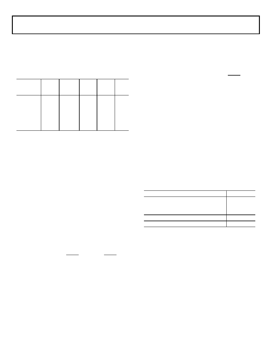
Table 4. Power Settings
Mode/State PLL
PLL
Bypassed
Core
Clock
(CCLK)
System
Clock
(SCLK)
Core
Power
Full On
Enabled
No
Enabled Enabled On
Active
Enabled/
Disabled
Yes
Enabled Enabled On
Sleep
Enabled
—
Disabled Enabled On
Deep Sleep
Disabled —
Disabled Disabled On
Hibernate
Disabled —
Disabled Disabled Off
Table 5. Power Domains
Power Domain
Power Supply
All internal logic, except Memory
VDDINT
Flash Memory
VDDFLASH
All other I/O
VDDEXT
ADC digital supply1 (Logic, I/O)
1 On ADSP-BF506F processor only.
DVDD, VDRIVE
ADC analog supply1
AVDD
Power Savings Factor
fCCLKRED
fCCLKNOM
--------------------------
VDDINTRED
VDDINTNOM
--------------------------------
2
×
TRED
TNOM
---------------
×
=
相关PDF资料 |
PDF描述 |
|---|---|
| ADSP-BF536BBCZ3BRL | IC DSP CTLR 16BIT 208BGA |
| ZWS240PAF36 | PWR SUP 36V 241.2W 6.7A |
| ZWS240PAF48 | PWR SUP 48V 240W 5A |
| MAX6501UKP125+T | IC TEMP SWITCH SOT23-5 |
| ZWQ1305223 | PWRSUP QUAD 5V/+12V/-12V/3.3V |
相关代理商/技术参数 |
参数描述 |
|---|---|
| ADSP-BF504KCPZ-4 | 功能描述:IC CCD SIGNAL PROCESSOR 88LFCSP RoHS:是 类别:集成电路 (IC) >> 嵌入式 - DSP(数字式信号处理器) 系列:Blackfin® 标准包装:2 系列:StarCore 类型:SC140 内核 接口:DSI,以太网,RS-232 时钟速率:400MHz 非易失内存:外部 芯片上RAM:1.436MB 电压 - 输入/输出:3.30V 电压 - 核心:1.20V 工作温度:-40°C ~ 105°C 安装类型:表面贴装 封装/外壳:431-BFBGA,FCBGA 供应商设备封装:431-FCPBGA(20x20) 包装:托盘 |
| ADSP-BF504KCPZ-4F | 功能描述:IC CCD SIGNAL PROCESSOR 88LFCSP RoHS:是 类别:集成电路 (IC) >> 嵌入式 - DSP(数字式信号处理器) 系列:Blackfin® 标准包装:2 系列:StarCore 类型:SC140 内核 接口:DSI,以太网,RS-232 时钟速率:400MHz 非易失内存:外部 芯片上RAM:1.436MB 电压 - 输入/输出:3.30V 电压 - 核心:1.20V 工作温度:-40°C ~ 105°C 安装类型:表面贴装 封装/外壳:431-BFBGA,FCBGA 供应商设备封装:431-FCPBGA(20x20) 包装:托盘 |
| ADSP-BF506BSWZ-3F | 功能描述:IC DSP 400MHZ 1.4V 120LQFP RoHS:是 类别:集成电路 (IC) >> 嵌入式 - DSP(数字式信号处理器) 系列:Blackfin® 标准包装:40 系列:TMS320DM64x, DaVinci™ 类型:定点 接口:I²C,McASP,McBSP 时钟速率:400MHz 非易失内存:外部 芯片上RAM:160kB 电压 - 输入/输出:3.30V 电压 - 核心:1.20V 工作温度:0°C ~ 90°C 安装类型:表面贴装 封装/外壳:548-BBGA,FCBGA 供应商设备封装:548-FCBGA(27x27) 包装:托盘 配用:TMDSDMK642-0E-ND - DEVELPER KIT W/NTSC CAMERA296-23038-ND - DSP STARTER KIT FOR TMS320C6416296-23059-ND - FLASHBURN PORTING KIT296-23058-ND - EVAL MODULE FOR DM642TMDSDMK642-ND - DEVELOPER KIT W/NTSC CAMERA |
| ADSP-BF506BSWZ-4F | 功能描述:IC DSP 400MHZ 1.4V 120LQFP RoHS:是 类别:集成电路 (IC) >> 嵌入式 - DSP(数字式信号处理器) 系列:Blackfin® 标准包装:40 系列:TMS320DM64x, DaVinci™ 类型:定点 接口:I²C,McASP,McBSP 时钟速率:400MHz 非易失内存:外部 芯片上RAM:160kB 电压 - 输入/输出:3.30V 电压 - 核心:1.20V 工作温度:0°C ~ 90°C 安装类型:表面贴装 封装/外壳:548-BBGA,FCBGA 供应商设备封装:548-FCBGA(27x27) 包装:托盘 配用:TMDSDMK642-0E-ND - DEVELPER KIT W/NTSC CAMERA296-23038-ND - DSP STARTER KIT FOR TMS320C6416296-23059-ND - FLASHBURN PORTING KIT296-23058-ND - EVAL MODULE FOR DM642TMDSDMK642-ND - DEVELOPER KIT W/NTSC CAMERA |
| ADSP-BF506BSWZ-4FX | 制造商:Analog Devices 功能描述:- Trays |
发布紧急采购,3分钟左右您将得到回复。