- 您现在的位置:买卖IC网 > PDF目录19388 > ADSP-BF537BBC-5A (Analog Devices Inc)IC DSP CTLR 16BIT 182CSPBGA PDF资料下载
参数资料
| 型号: | ADSP-BF537BBC-5A |
| 厂商: | Analog Devices Inc |
| 文件页数: | 11/68页 |
| 文件大小: | 0K |
| 描述: | IC DSP CTLR 16BIT 182CSPBGA |
| 产品培训模块: | Blackfin® Processor Core Architecture Overview Blackfin® Device Drivers Blackfin® Optimizations for Performance and Power Consumption Blackfin® System Services |
| 标准包装: | 1 |
| 系列: | Blackfin® |
| 类型: | 定点 |
| 接口: | CAN,SPI,SSP,TWI,UART |
| 时钟速率: | 500MHz |
| 非易失内存: | 外部 |
| 芯片上RAM: | 132kB |
| 电压 - 输入/输出: | 2.50V,3.30V |
| 电压 - 核心: | 1.26V |
| 工作温度: | -40°C ~ 85°C |
| 安装类型: | 表面贴装 |
| 封装/外壳: | 182-LFBGA,CSPBGA |
| 供应商设备封装: | 182-CSPBGA(12x12) |
| 包装: | 托盘 |
| 配用: | ADZS-BF537-ASKIT-ND - BOARD EVAL SKIT ADSP-BF537 ADZS-BFAUDIO-EZEXT-ND - BOARD EVAL AUDIO BLACKFIN ADZS-BF537-EZLITE-ND - BOARD EVAL ADSP-BF537 ADZS-BFAV-EZEXT-ND - BOARD DAUGHT ADSP-BF533,37,61KIT ADZS-BF537-STAMP-ND - SYSTEM DEV FOR ADSP-BF537 |
第1页第2页第3页第4页第5页第6页第7页第8页第9页第10页当前第11页第12页第13页第14页第15页第16页第17页第18页第19页第20页第21页第22页第23页第24页第25页第26页第27页第28页第29页第30页第31页第32页第33页第34页第35页第36页第37页第38页第39页第40页第41页第42页第43页第44页第45页第46页第47页第48页第49页第50页第51页第52页第53页第54页第55页第56页第57页第58页第59页第60页第61页第62页第63页第64页第65页第66页第67页第68页
Rev. J
|
Page 19 of 68
|
February 2014
PIN DESCRIPTIONS
The ADSP-BF534/ADSP-BF536/ADSP-BF537 processors pin
definitions are listed in Table 9. In order to maintain maximum
functionality and reduce package size and pin count, some pins
have dual, multiplexed functions. In cases where pin function is
reconfigurable, the default state is shown in plain text, while the
alternate function is shown in italics. Pins shown with an aster-
isk after their name (*) offer high source/high sink current
capabilities.
All pins are three-stated during and immediately after reset,
with the exception of the external memory interface, asynchro-
nous and synchronous memory control, and the buffered XTAL
output pin (CLKBUF). On the external memory interface, the
control and address lines are driven high, with the exception of
CLKOUT, which toggles at the system clock rate. If BR is active
(whether or not RESET is asserted), the memory pins are also
three-stated. During hibernate, all outputs are three-stated
unless otherwise noted in Table 9.
All I/O pins have their input buffers disabled with the exception
of the pins noted in the data sheet that need pull-ups or pull-
downs if unused.
The SDA (serial data) and SCL (serial clock) pins are open drain
and therefore require a pull-up resistor. Consult version 2.1 of
the I2C specification for the proper resistor value.
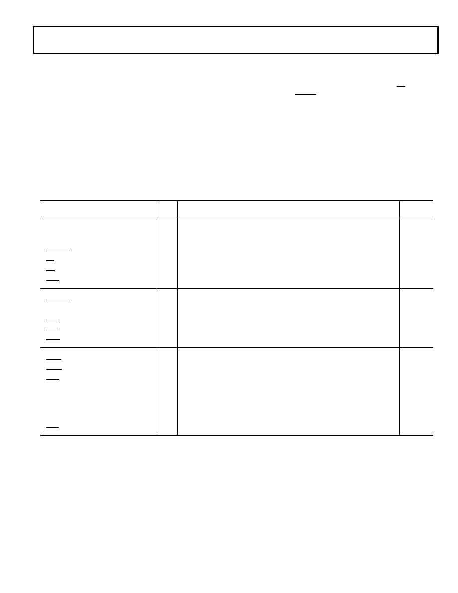
Table 9. Pin Descriptions
Pin Name
Type Function
Driver
Type1
Memory Interface
ADDR19–1
O
Address Bus for Async Access
A
DATA15–0
I/O
Data Bus for Async/Sync Access
A
ABE1–0/SDQM1–0
O
Byte Enables/Data Masks for Async/Sync Access
A
BR
I
Bus Request (This pin should be pulled high when not used.)
BG
OBus Grant
A
BGH
O
Bus Grant Hang
A
Asynchronous Memory Control
AMS3–0
O
Bank Select (Require pull-ups if hibernate is used.)
A
ARDY
I
Hardware Ready Control
AOE
O
Output Enable
A
ARE
ORead Enable
A
AWE
OWrite Enable
A
Synchronous Memory Control
SRAS
O
Row Address Strobe
A
SCAS
O
Column Address Strobe
A
SWE
OWrite Enable
A
SCKE
O
Clock Enable(Requires a pull-down if hibernate with SDRAM self-refresh is
used.)
A
CLKOUT
O
Clock Output
B
SA10
O
A10 Pin
A
SMS
OBank Select
A
相关PDF资料 |
PDF描述 |
|---|---|
| MC78L18ACP | IC REG LDO 18V .1A TO92 |
| TPSC107M010R0150 | CAP TANT 100UF 10V 20% 2312 |
| MC78L15ACP | IC REG LDO 15V .1A TO92 |
| MC78L12ACP | IC REG LDO 12V .1A TO92 |
| MC78L12ABP | IC REG LDO 12V .1A TO92 |
相关代理商/技术参数 |
参数描述 |
|---|---|
| ADSP-BF537BBC-5AV | 制造商:Rochester Electronics LLC 功能描述: 制造商:Analog Devices 功能描述: |
| ADSP-BF537BBCZ-5A | 功能描述:数字信号处理器和控制器 - DSP, DSC Blackfin processor 500MHz 132KB SRAM RoHS:否 制造商:Microchip Technology 核心:dsPIC 数据总线宽度:16 bit 程序存储器大小:16 KB 数据 RAM 大小:2 KB 最大时钟频率:40 MHz 可编程输入/输出端数量:35 定时器数量:3 设备每秒兆指令数:50 MIPs 工作电源电压:3.3 V 最大工作温度:+ 85 C 封装 / 箱体:TQFP-44 安装风格:SMD/SMT |
| ADSP-BF537BBCZ-5A | 制造商:Analog Devices 功能描述:Digital Signal Processor IC |
| ADSP-BF537BBCZ-5AV | 功能描述:IC DSP CTLR 16BIT 182CSPBGA RoHS:是 类别:集成电路 (IC) >> 嵌入式 - DSP(数字式信号处理器) 系列:Blackfin® 标准包装:2 系列:StarCore 类型:SC140 内核 接口:DSI,以太网,RS-232 时钟速率:400MHz 非易失内存:外部 芯片上RAM:1.436MB 电压 - 输入/输出:3.30V 电压 - 核心:1.20V 工作温度:-40°C ~ 105°C 安装类型:表面贴装 封装/外壳:431-BFBGA,FCBGA 供应商设备封装:431-FCPBGA(20x20) 包装:托盘 |
| ADSP-BF537BBCZ-5AV | 制造商:Analog Devices 功能描述:Digital Signal Processor IC |
发布紧急采购,3分钟左右您将得到回复。