- 您现在的位置:买卖IC网 > PDF目录19388 > ADSP-BF537BBC-5A (Analog Devices Inc)IC DSP CTLR 16BIT 182CSPBGA PDF资料下载
参数资料
| 型号: | ADSP-BF537BBC-5A |
| 厂商: | Analog Devices Inc |
| 文件页数: | 24/68页 |
| 文件大小: | 0K |
| 描述: | IC DSP CTLR 16BIT 182CSPBGA |
| 产品培训模块: | Blackfin® Processor Core Architecture Overview Blackfin® Device Drivers Blackfin® Optimizations for Performance and Power Consumption Blackfin® System Services |
| 标准包装: | 1 |
| 系列: | Blackfin® |
| 类型: | 定点 |
| 接口: | CAN,SPI,SSP,TWI,UART |
| 时钟速率: | 500MHz |
| 非易失内存: | 外部 |
| 芯片上RAM: | 132kB |
| 电压 - 输入/输出: | 2.50V,3.30V |
| 电压 - 核心: | 1.26V |
| 工作温度: | -40°C ~ 85°C |
| 安装类型: | 表面贴装 |
| 封装/外壳: | 182-LFBGA,CSPBGA |
| 供应商设备封装: | 182-CSPBGA(12x12) |
| 包装: | 托盘 |
| 配用: | ADZS-BF537-ASKIT-ND - BOARD EVAL SKIT ADSP-BF537 ADZS-BFAUDIO-EZEXT-ND - BOARD EVAL AUDIO BLACKFIN ADZS-BF537-EZLITE-ND - BOARD EVAL ADSP-BF537 ADZS-BFAV-EZEXT-ND - BOARD DAUGHT ADSP-BF533,37,61KIT ADZS-BF537-STAMP-ND - SYSTEM DEV FOR ADSP-BF537 |
第1页第2页第3页第4页第5页第6页第7页第8页第9页第10页第11页第12页第13页第14页第15页第16页第17页第18页第19页第20页第21页第22页第23页当前第24页第25页第26页第27页第28页第29页第30页第31页第32页第33页第34页第35页第36页第37页第38页第39页第40页第41页第42页第43页第44页第45页第46页第47页第48页第49页第50页第51页第52页第53页第54页第55页第56页第57页第58页第59页第60页第61页第62页第63页第64页第65页第66页第67页第68页
Rev. J
|
Page 30 of 68
|
February 2014
TIMING SPECIFICATIONS
Component specifications are subject to change
without notice.
Clock and Reset Timing
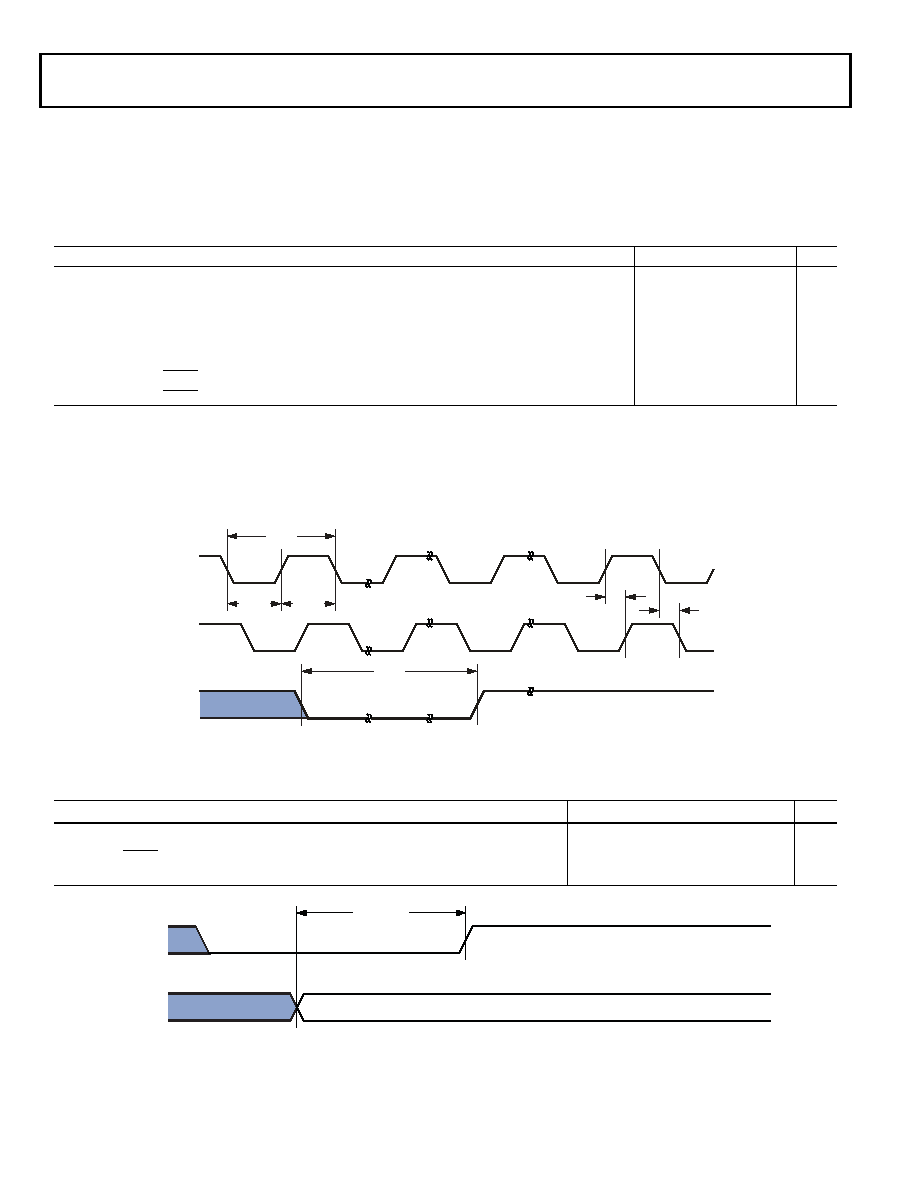
Table 22. Clock Input and Reset Timing
Parameter
Min
Max
Unit
Timing Requirements
tCKIN
CLKIN Period1, 2, 3, 4
1 Combinations of the CLKIN frequency and the PLL clock multiplier must not exceed the allowed fVCO, fCCLK, and fSCLK settings discussed in Table 10 through Table 14. Since
by default the PLL is multiplying the CLKIN frequency by 10 MHz, 300 MHz, and 400 MHz speed grade parts can not use the full CLKIN period range.
2 Applies to PLL bypass mode and PLL non bypass mode.
3 CLKIN frequency must not change on the fly.
4 If the DF bit in the PLL_CTL register is set, then the maximum t
CKIN period is 50 ns.
20.0
100.0
ns
tCKINL
CLKIN Low Pulse
8.0
ns
tCKINH
CLKIN High Pulse
8.0
ns
tBUFDLAY
CLKIN to CLKBUF Delay
10
ns
tWRST
RESET Asserted Pulse Width Low
11 × tCKIN
ns
tNOBOOT
RESET Deassertion to First External Access Delay5
5 Applies when processor is configured in No Boot Mode (BMODE2-0 = b#000).
3 × tCKIN
5 × tCKIN
ns
Figure 9. Clock and Reset Timing
Table 23. Power-Up Reset Timing
Parameter
Min
Max
Unit
Timing Requirements
tRST_IN_PWR
RESET Deasserted After the VDDINT, VDDEXT, VDDRTC, and CLKIN Pins Are Stable and
Within Specification
3500 × tCKIN
ns
Figure 10. Power-Up Reset Timing
CLKIN
tWRST
tCKIN
tCKINL
tCKINH
tBUFDLAY
RESET
CLKBUF
RESET
tRST_IN_PWR
CLKIN
V
DD_SUPPLIES
相关PDF资料 |
PDF描述 |
|---|---|
| MC78L18ACP | IC REG LDO 18V .1A TO92 |
| TPSC107M010R0150 | CAP TANT 100UF 10V 20% 2312 |
| MC78L15ACP | IC REG LDO 15V .1A TO92 |
| MC78L12ACP | IC REG LDO 12V .1A TO92 |
| MC78L12ABP | IC REG LDO 12V .1A TO92 |
相关代理商/技术参数 |
参数描述 |
|---|---|
| ADSP-BF537BBC-5AV | 制造商:Rochester Electronics LLC 功能描述: 制造商:Analog Devices 功能描述: |
| ADSP-BF537BBCZ-5A | 功能描述:数字信号处理器和控制器 - DSP, DSC Blackfin processor 500MHz 132KB SRAM RoHS:否 制造商:Microchip Technology 核心:dsPIC 数据总线宽度:16 bit 程序存储器大小:16 KB 数据 RAM 大小:2 KB 最大时钟频率:40 MHz 可编程输入/输出端数量:35 定时器数量:3 设备每秒兆指令数:50 MIPs 工作电源电压:3.3 V 最大工作温度:+ 85 C 封装 / 箱体:TQFP-44 安装风格:SMD/SMT |
| ADSP-BF537BBCZ-5A | 制造商:Analog Devices 功能描述:Digital Signal Processor IC |
| ADSP-BF537BBCZ-5AV | 功能描述:IC DSP CTLR 16BIT 182CSPBGA RoHS:是 类别:集成电路 (IC) >> 嵌入式 - DSP(数字式信号处理器) 系列:Blackfin® 标准包装:2 系列:StarCore 类型:SC140 内核 接口:DSI,以太网,RS-232 时钟速率:400MHz 非易失内存:外部 芯片上RAM:1.436MB 电压 - 输入/输出:3.30V 电压 - 核心:1.20V 工作温度:-40°C ~ 105°C 安装类型:表面贴装 封装/外壳:431-BFBGA,FCBGA 供应商设备封装:431-FCPBGA(20x20) 包装:托盘 |
| ADSP-BF537BBCZ-5AV | 制造商:Analog Devices 功能描述:Digital Signal Processor IC |
发布紧急采购,3分钟左右您将得到回复。