- 您现在的位置:买卖IC网 > PDF目录19388 > ADSP-BF537BBC-5A (Analog Devices Inc)IC DSP CTLR 16BIT 182CSPBGA PDF资料下载
参数资料
| 型号: | ADSP-BF537BBC-5A |
| 厂商: | Analog Devices Inc |
| 文件页数: | 56/68页 |
| 文件大小: | 0K |
| 描述: | IC DSP CTLR 16BIT 182CSPBGA |
| 产品培训模块: | Blackfin® Processor Core Architecture Overview Blackfin® Device Drivers Blackfin® Optimizations for Performance and Power Consumption Blackfin® System Services |
| 标准包装: | 1 |
| 系列: | Blackfin® |
| 类型: | 定点 |
| 接口: | CAN,SPI,SSP,TWI,UART |
| 时钟速率: | 500MHz |
| 非易失内存: | 外部 |
| 芯片上RAM: | 132kB |
| 电压 - 输入/输出: | 2.50V,3.30V |
| 电压 - 核心: | 1.26V |
| 工作温度: | -40°C ~ 85°C |
| 安装类型: | 表面贴装 |
| 封装/外壳: | 182-LFBGA,CSPBGA |
| 供应商设备封装: | 182-CSPBGA(12x12) |
| 包装: | 托盘 |
| 配用: | ADZS-BF537-ASKIT-ND - BOARD EVAL SKIT ADSP-BF537 ADZS-BFAUDIO-EZEXT-ND - BOARD EVAL AUDIO BLACKFIN ADZS-BF537-EZLITE-ND - BOARD EVAL ADSP-BF537 ADZS-BFAV-EZEXT-ND - BOARD DAUGHT ADSP-BF533,37,61KIT ADZS-BF537-STAMP-ND - SYSTEM DEV FOR ADSP-BF537 |
第1页第2页第3页第4页第5页第6页第7页第8页第9页第10页第11页第12页第13页第14页第15页第16页第17页第18页第19页第20页第21页第22页第23页第24页第25页第26页第27页第28页第29页第30页第31页第32页第33页第34页第35页第36页第37页第38页第39页第40页第41页第42页第43页第44页第45页第46页第47页第48页第49页第50页第51页第52页第53页第54页第55页当前第56页第57页第58页第59页第60页第61页第62页第63页第64页第65页第66页第67页第68页
Rev. J
|
Page 6 of 68
|
February 2014
memory space, the processor starts executing from the on-chip
boot ROM. For more information, see Booting Modes on
Event Handling
The event controller on the Blackfin processor handles all asyn-
chronous and synchronous events to the processor. The
Blackfin processor provides event handling that supports both
nesting and prioritization. Nesting allows multiple event service
routines to be active simultaneously. Prioritization ensures that
servicing of a higher priority event takes precedence over servic-
ing of a lower priority event. The controller provides support for
five different types of events:
Emulation – An emulation event causes the processor to
enter emulation mode, allowing command and control of
the processor via the JTAG interface.
Reset – This event resets the processor.
Nonmaskable Interrupt (NMI) – The NMI event can be
generated by the software watchdog timer or by the NMI
input signal to the processor. The NMI event is frequently
used as a power-down indicator to initiate an orderly shut-
down of the system.
Exceptions – Events that occur synchronously to program
flow (in other words, the exception is taken before the
instruction is allowed to complete). Conditions such as
data alignment violations and undefined instructions cause
exceptions.
Interrupts – Events that occur asynchronously to program
flow. They are caused by input pins, timers, and other
peripherals, as well as by an explicit software instruction.
Each event type has an associated register to hold the return
address and an associated return-from-event instruction. When
an event is triggered, the state of the processor is saved on the
supervisor stack.
The Blackfin processor event controller consists of two stages:
the core event controller (CEC) and the system interrupt con-
troller (SIC). The core event controller works with the system
interrupt controller to prioritize and control all system events.
Conceptually, interrupts from the peripherals enter into the
SIC, and are then routed directly into the general-purpose inter-
rupts of the CEC.
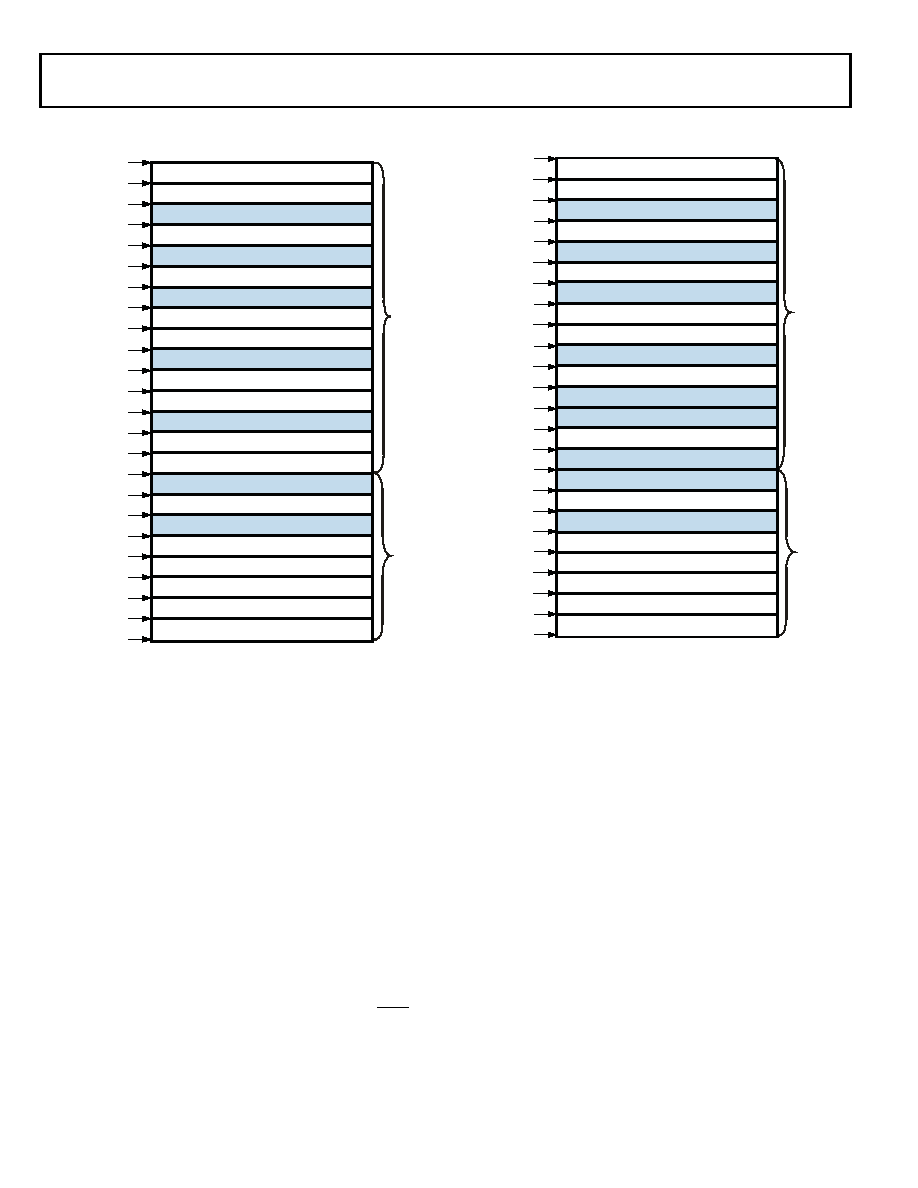
Figure 3. ADSP-BF534/ADSP-BF536/ADSP-BF537 Memory Maps
RESERVED
CORE MMR REGISTERS (2M BYTES)
RESERVED
SCRATCHPAD SRAM (4K BYTES)
INSTRUCTION BANK B SRAM (16K BYTES)
SYSTEM MMR REGISTERS (2M BYTES)
RESERVED
DATA BANK B SRAM/CACHE (16K BYTES)
DATA BANK B SRAM (16K BYTES)
DATA BANK A SRAM/CACHE (16K BYTES)
ASYNC MEMORY BANK 3 (1M BYTES)
ASYNC MEMORY BANK 2 (1M BYTES)
ASYNC MEMORY BANK 1 (1M BYTES)
ASYNC MEMORY BANK 0 (1M BYTES)
SDRAM MEMORY (16M BYTES TO 512M BYTES)
INSTRUCTION SRAM/CACHE (16K BYTES)
IN
TE
R
N
AL
M
E
M
O
RY
M
A
P
EX
T
E
R
NA
L
M
E
MO
R
YM
A
P
0xFFFF FFFF
0xFFE0 0000
0xFFB0 0000
0xFFA1 4000
0xFFA1 0000
0xFF90 8000
0xFF90 4000
0xFF80 8000
0xFF80 4000
0x2040 0000
0x2030 0000
0x2020 0000
0x2010 0000
0x2000 0000
0xEF00 0000
0x0000 0000
0xFFC0 0000
0xFFB0 1000
0xFFA0 0000
DATA BANK A SRAM (16K BYTES)
0xFF90 0000
0xFF80 0000
RESERVED
0xFFA0 C000
0xFFA0 8000
INSTRUCTION BANK A SRAM (32K BYTES)
RESERVED
BOOT ROM (2K BYTES)
0xEF00 0800
ADSP-BF534/ADSP-BF537 MEMORY MAP
RESERVED
CORE MMR REGISTERS (2M BYTES)
RESERVED
SCRATCHPAD SRAM (4K BYTES)
INSTRUCTION BANK B SRAM (16K BYTES)
SYSTEM MMR REGISTERS (2M BYTES)
RESERVED
DATA BANK B SRAM/CACHE (16K BYTES)
DATA BANK A SRAM/CACHE (16K BYTES)
ASYNC MEMORY BANK 3 (1M BYTES)
ASYNC MEMORY BANK 2 (1M BYTES)
ASYNC MEMORY BANK 1 (1M BYTES)
ASYNCMEMORY BANK0 (1M BYTES)
SDRAM MEMORY (16M BYTES TO 512M BYTES)
INSTRUCTION SRAM/CACHE (16K BYTES)
IN
TE
R
N
A
L
M
E
M
O
R
Y
M
A
P
E
X
TE
R
N
AL
ME
M
O
R
Y
M
AP
0xFFFF FFFF
0xFFE0 0000
0xFFB0 0000
0xFFA1 4000
0xFFA1 0000
0xFF90 8000
0xFF90 4000
0xFF80 8000
0xFF80 4000
0x2040 0000
0x2030 0000
0x2020 0000
0x2010 0000
0x2000 0000
0xEF00 0000
0x0000 0000
0xFFC0 0000
0xFFB0 1000
0xFFA0 0000
0xFF90 0000
0xFF80 0000
RESERVED
0xFFA0 C000
0xFFA0 8000
INSTRUCTION BANK A SRAM (32K BYTES)
RESERVED
BOOT ROM (2K BYTES)
0xEF00 0800
ADSP-BF536 MEMORY MAP
相关PDF资料 |
PDF描述 |
|---|---|
| MC78L18ACP | IC REG LDO 18V .1A TO92 |
| TPSC107M010R0150 | CAP TANT 100UF 10V 20% 2312 |
| MC78L15ACP | IC REG LDO 15V .1A TO92 |
| MC78L12ACP | IC REG LDO 12V .1A TO92 |
| MC78L12ABP | IC REG LDO 12V .1A TO92 |
相关代理商/技术参数 |
参数描述 |
|---|---|
| ADSP-BF537BBC-5AV | 制造商:Rochester Electronics LLC 功能描述: 制造商:Analog Devices 功能描述: |
| ADSP-BF537BBCZ-5A | 功能描述:数字信号处理器和控制器 - DSP, DSC Blackfin processor 500MHz 132KB SRAM RoHS:否 制造商:Microchip Technology 核心:dsPIC 数据总线宽度:16 bit 程序存储器大小:16 KB 数据 RAM 大小:2 KB 最大时钟频率:40 MHz 可编程输入/输出端数量:35 定时器数量:3 设备每秒兆指令数:50 MIPs 工作电源电压:3.3 V 最大工作温度:+ 85 C 封装 / 箱体:TQFP-44 安装风格:SMD/SMT |
| ADSP-BF537BBCZ-5A | 制造商:Analog Devices 功能描述:Digital Signal Processor IC |
| ADSP-BF537BBCZ-5AV | 功能描述:IC DSP CTLR 16BIT 182CSPBGA RoHS:是 类别:集成电路 (IC) >> 嵌入式 - DSP(数字式信号处理器) 系列:Blackfin® 标准包装:2 系列:StarCore 类型:SC140 内核 接口:DSI,以太网,RS-232 时钟速率:400MHz 非易失内存:外部 芯片上RAM:1.436MB 电压 - 输入/输出:3.30V 电压 - 核心:1.20V 工作温度:-40°C ~ 105°C 安装类型:表面贴装 封装/外壳:431-BFBGA,FCBGA 供应商设备封装:431-FCPBGA(20x20) 包装:托盘 |
| ADSP-BF537BBCZ-5AV | 制造商:Analog Devices 功能描述:Digital Signal Processor IC |
发布紧急采购,3分钟左右您将得到回复。