- 您现在的位置:买卖IC网 > PDF目录19388 > ADSP-BF537BBC-5A (Analog Devices Inc)IC DSP CTLR 16BIT 182CSPBGA PDF资料下载
参数资料
| 型号: | ADSP-BF537BBC-5A |
| 厂商: | Analog Devices Inc |
| 文件页数: | 48/68页 |
| 文件大小: | 0K |
| 描述: | IC DSP CTLR 16BIT 182CSPBGA |
| 产品培训模块: | Blackfin® Processor Core Architecture Overview Blackfin® Device Drivers Blackfin® Optimizations for Performance and Power Consumption Blackfin® System Services |
| 标准包装: | 1 |
| 系列: | Blackfin® |
| 类型: | 定点 |
| 接口: | CAN,SPI,SSP,TWI,UART |
| 时钟速率: | 500MHz |
| 非易失内存: | 外部 |
| 芯片上RAM: | 132kB |
| 电压 - 输入/输出: | 2.50V,3.30V |
| 电压 - 核心: | 1.26V |
| 工作温度: | -40°C ~ 85°C |
| 安装类型: | 表面贴装 |
| 封装/外壳: | 182-LFBGA,CSPBGA |
| 供应商设备封装: | 182-CSPBGA(12x12) |
| 包装: | 托盘 |
| 配用: | ADZS-BF537-ASKIT-ND - BOARD EVAL SKIT ADSP-BF537 ADZS-BFAUDIO-EZEXT-ND - BOARD EVAL AUDIO BLACKFIN ADZS-BF537-EZLITE-ND - BOARD EVAL ADSP-BF537 ADZS-BFAV-EZEXT-ND - BOARD DAUGHT ADSP-BF533,37,61KIT ADZS-BF537-STAMP-ND - SYSTEM DEV FOR ADSP-BF537 |
第1页第2页第3页第4页第5页第6页第7页第8页第9页第10页第11页第12页第13页第14页第15页第16页第17页第18页第19页第20页第21页第22页第23页第24页第25页第26页第27页第28页第29页第30页第31页第32页第33页第34页第35页第36页第37页第38页第39页第40页第41页第42页第43页第44页第45页第46页第47页当前第48页第49页第50页第51页第52页第53页第54页第55页第56页第57页第58页第59页第60页第61页第62页第63页第64页第65页第66页第67页第68页
Rev. J
|
Page 52 of 68
|
February 2014
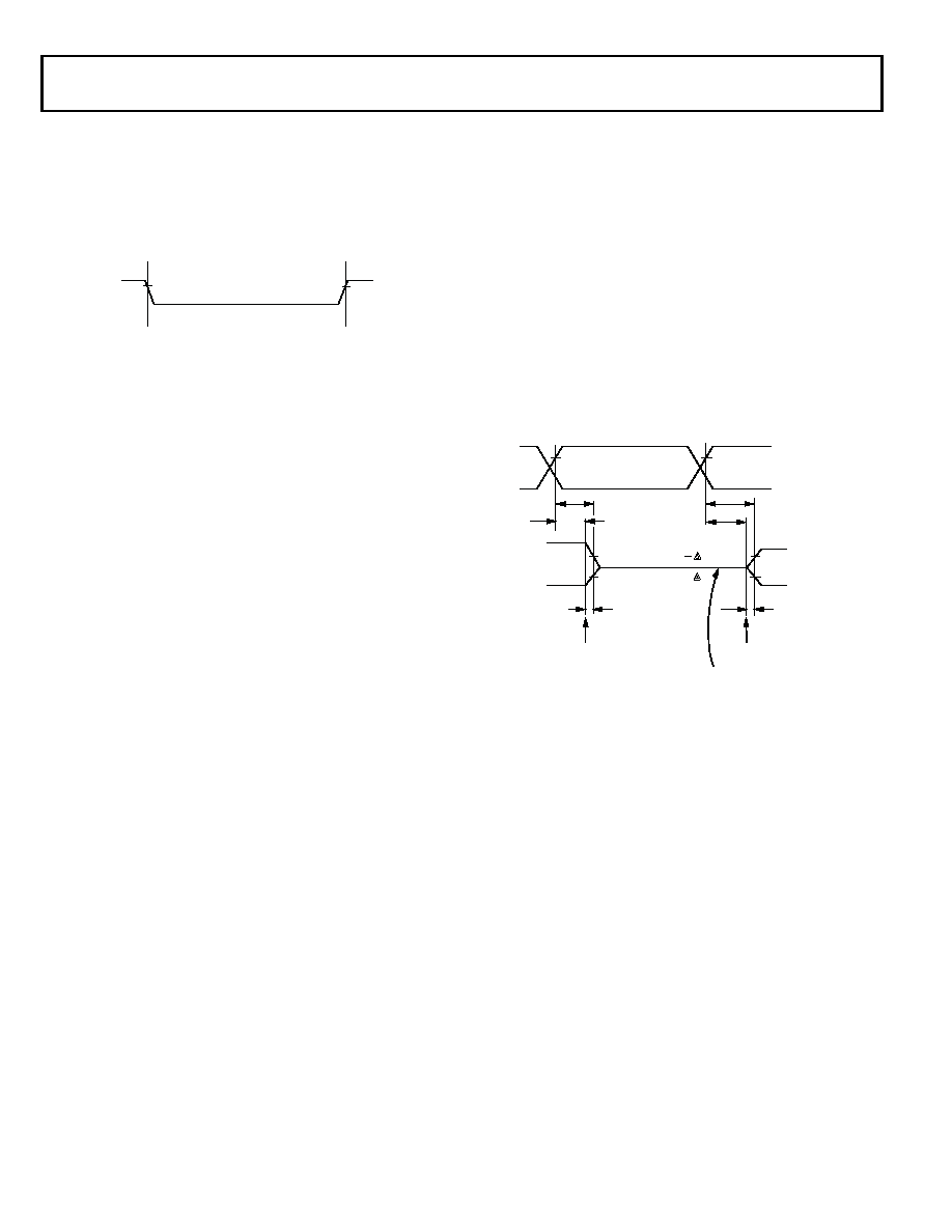
TEST CONDITIONS
All timing parameters appearing in this data sheet were
measured under the conditions described in this section.
Figure 48 shows the measurement point for ac measurements
(other than output enable/disable). The measurement point is
VMEAS = VDDEXT/2.
Output Enable Time
Output pins are considered to be enabled when they have made
a transition from a high impedance state to the point when they
start driving. The output enable time tENA is the interval from
the point when a reference signal reaches a high or low voltage
level to the point when the output starts driving as shown in the
Output Enable/Disable diagram (Figure 49). The time tENA_MEA-
SURED is the interval from when the reference signal switches to
when the output voltage reaches 2.0 V (output high) or 1.0 V
(output low). Time tTRIP is the interval from when the output
starts driving to when the output reaches the 1.0 V or 2.0 V trip
voltage. Time tENA is calculated as shown in
the equation:
If multiple pins (such as the data bus) are enabled, the measure-
ment value is that of the first pin to start driving.
Output Disable Time
Output pins are considered to be disabled when they stop driv-
ing, go into a high impedance state, and start to decay from their
output high or low voltage. The time for the voltage on the bus
to decay by V is dependent on the capacitive load, CL, and the
load current, IL. This decay time can be approximated by
the equation:
The output disable time tDIS is the difference between tDIS_MEA-
the interval from when the reference signal switches to when the
output voltage decays V from the measured output-high or
output-low voltage. The time tDECAY is calculated with the test
loads CL and IL, and with V equal to 0.5 V.
Example System Hold Time Calculation
To determine the data output hold time in a particular system,
first calculate tDECAY using the equation given above. Choose V
to be the difference between the processor’s output voltage and
the input threshold for the device requiring the hold time. A
typical V is 0.4 V. CL is the total bus capacitance (per data line),
and IL is the total leakage or three-state current (per data line).
The hold time is tDECAY plus the minimum disable time (for
example, tDSDAT for an SDRAM write cycle).
Figure 48. Voltage Reference Levels for AC Measurements (Except
Output Enable/Disable)
INPUT
OR
OUTPUT
VMEAS
tENA
tENA_MEASURED tTRIP
–
=
Figure 49. Output Enable/Disable
tDECAY
CL V
I
L
=
REFERENCE
SIGNAL
tDIS
OUTPUT STARTS DRIVING
VOH (MEASURED)
V
VOL (MEASURED) + V
tDIS_MEASURED
VOH
(MEASURED)
VOL
(MEASURED)
VTRIP(HIGH)
VOH(MEASURED)
VOL(MEASURED)
HIGH IMPEDANCE STATE
OUTPUT STOPS DRIVING
tENA
tDECAY
tENA_MEASURED
tTRIP
VTRIP(LOW)
相关PDF资料 |
PDF描述 |
|---|---|
| MC78L18ACP | IC REG LDO 18V .1A TO92 |
| TPSC107M010R0150 | CAP TANT 100UF 10V 20% 2312 |
| MC78L15ACP | IC REG LDO 15V .1A TO92 |
| MC78L12ACP | IC REG LDO 12V .1A TO92 |
| MC78L12ABP | IC REG LDO 12V .1A TO92 |
相关代理商/技术参数 |
参数描述 |
|---|---|
| ADSP-BF537BBC-5AV | 制造商:Rochester Electronics LLC 功能描述: 制造商:Analog Devices 功能描述: |
| ADSP-BF537BBCZ-5A | 功能描述:数字信号处理器和控制器 - DSP, DSC Blackfin processor 500MHz 132KB SRAM RoHS:否 制造商:Microchip Technology 核心:dsPIC 数据总线宽度:16 bit 程序存储器大小:16 KB 数据 RAM 大小:2 KB 最大时钟频率:40 MHz 可编程输入/输出端数量:35 定时器数量:3 设备每秒兆指令数:50 MIPs 工作电源电压:3.3 V 最大工作温度:+ 85 C 封装 / 箱体:TQFP-44 安装风格:SMD/SMT |
| ADSP-BF537BBCZ-5A | 制造商:Analog Devices 功能描述:Digital Signal Processor IC |
| ADSP-BF537BBCZ-5AV | 功能描述:IC DSP CTLR 16BIT 182CSPBGA RoHS:是 类别:集成电路 (IC) >> 嵌入式 - DSP(数字式信号处理器) 系列:Blackfin® 标准包装:2 系列:StarCore 类型:SC140 内核 接口:DSI,以太网,RS-232 时钟速率:400MHz 非易失内存:外部 芯片上RAM:1.436MB 电压 - 输入/输出:3.30V 电压 - 核心:1.20V 工作温度:-40°C ~ 105°C 安装类型:表面贴装 封装/外壳:431-BFBGA,FCBGA 供应商设备封装:431-FCPBGA(20x20) 包装:托盘 |
| ADSP-BF537BBCZ-5AV | 制造商:Analog Devices 功能描述:Digital Signal Processor IC |
发布紧急采购,3分钟左右您将得到回复。