- 您现在的位置:买卖IC网 > PDF目录12018 > ADUC812BSZ (Analog Devices Inc)IC ADC 12BIT MULTICH MCU 52-MQFP PDF资料下载
参数资料
| 型号: | ADUC812BSZ |
| 厂商: | Analog Devices Inc |
| 文件页数: | 15/57页 |
| 文件大小: | 0K |
| 描述: | IC ADC 12BIT MULTICH MCU 52-MQFP |
| 产品培训模块: | Process Control |
| 标准包装: | 1 |
| 系列: | MicroConverter® ADuC8xx |
| 核心处理器: | 8052 |
| 芯体尺寸: | 8-位 |
| 速度: | 16MHz |
| 连通性: | I²C,SPI,UART/USART |
| 外围设备: | PSM,温度传感器,WDT |
| 输入/输出数: | 34 |
| 程序存储器容量: | 8KB(8K x 8) |
| 程序存储器类型: | 闪存 |
| EEPROM 大小: | 640 x 8 |
| RAM 容量: | 256 x 8 |
| 电压 - 电源 (Vcc/Vdd): | 2.7 V ~ 5.5 V |
| 数据转换器: | A/D 8x12b,D/A 2x12b |
| 振荡器型: | 内部 |
| 工作温度: | -40°C ~ 85°C |
| 封装/外壳: | 52-QFP |
| 包装: | 托盘 |
| 产品目录页面: | 738 (CN2011-ZH PDF) |
第1页第2页第3页第4页第5页第6页第7页第8页第9页第10页第11页第12页第13页第14页当前第15页第16页第17页第18页第19页第20页第21页第22页第23页第24页第25页第26页第27页第28页第29页第30页第31页第32页第33页第34页第35页第36页第37页第38页第39页第40页第41页第42页第43页第44页第45页第46页第47页第48页第49页第50页第51页第52页第53页第54页第55页第56页第57页
REV.
ADuC812
–22–
Using the DAC
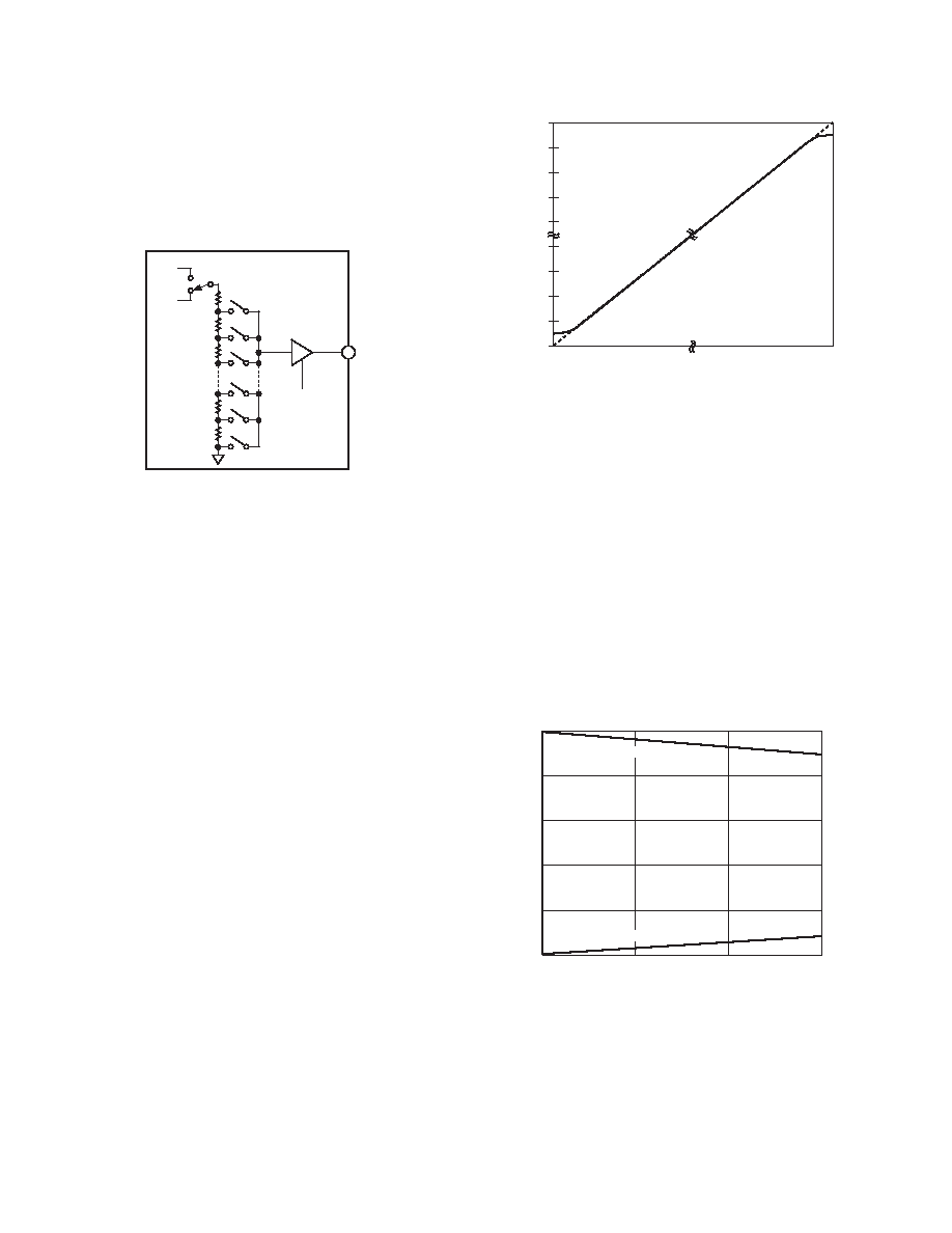
The on-chip DAC architecture consists of a resistor string DAC
followed by an output buffer amplifier, the functional equivalent
of which is illustrated in Figure 18. Details of the actual DAC
architecture can be found in U.S. Patent Number 5969657
(www.uspto.gov). Features of this architecture include inherent
guaranteed monotonicity and excellent differential linearity.
ADuC812
AVDD
VREF
R
OUTPUT
BUFFER
8
R
HIGH-Z
DISABLE
(FROM MCU)
Figure 18. Resistor String DAC Functional Equivalent
As illustrated in Figure 18, the reference source for each DAC is
user selectable in software. It can be either AVDD or VREF. In
0-to-AVDD mode, the DAC output transfer function spans from
0 V to the voltage at the AVDD pin. In 0-to-VREF mode, the
DAC output transfer function spans from 0 V to the internal
VREF, or if an external reference is applied, the voltage at the
VREF pin. The DAC output buffer amplifier features a true rail-to-
rail output stage implementation. This means that unloaded, each
output is capable of swinging to within less than 100 mV of both
AVDD and ground. Moreover, the DAC’s linearity specification
(when driving a 10 k
Ω resistive load to ground) is guaranteed
through the full transfer function except codes 0 to 48, and, in
0-to-AVDD mode only, codes 3995 to 4095. Linearity degradation
near ground and VDD is caused by saturation of the output
amplifier, and a general representation of its effects (neglecting
offset and gain error) is illustrated in Figure 19. The dotted line
in Figure 19 indicates the ideal transfer function, and the solid
line represents what the transfer function might look like with
endpoint nonlinearities due to saturation of the output amplifier. Note
that Figure 19 represents a transfer function in 0-to-VDD mode
only. In 0-to-VREF mode (with VREF < VDD) the lower nonlinearity
would be similar, but the upper portion of the transfer function
would follow the “ideal” line right to the end (VREF in this case,
not VDD), showing no signs of endpoint linearity errors.
VDD
FFF HEX
000 HEX
VDD – 50mV
VDD – 100mV
100mV
50mV
0mV
Figure 19. Endpoint Nonlinearities Due to Amplifier
Saturation
The endpoint nonlinearities conceptually illustrated in Figure 19
get worse as a function of output loading. Most of the ADuC812’s
data sheet specifications assume a 10 k
Ω resistive load to ground
at the DAC output. As the output is forced to source or sink
more current, the nonlinear regions at the top or bottom
(respectively) of Figure 19 become larger. With larger current
demands, this can significantly limit output voltage swing.
Figure 20 and Figure 21 illustrate this behavior. It should be noted
that the upper trace in each of these figures is only valid for an
output range selection of 0-to-AVDD. In 0-to-VREF mode, DAC
loading will not cause high-side voltage drops as long as the
reference voltage remains below the upper trace in the correspond-
ing figure. For example, if AVDD = 3 V and VREF = 2.5 V, the
high-side voltage will not be affected by loads less than 5 mA.
But somewhere around 7 mA the upper curve in Figure 21 drops
below 2.5 V (VREF), indicating that at these higher currents the
output will not be capable of reaching VREF.
SOURCE/SINK CURRENT – mA
5
05
10
15
OUTPUT
VOLTAGE
–
V
4
3
2
1
0
DAC LOADED WITH 0FFF HEX
DAC LOADED WITH 0000 HEX
Figure 20. Source and Sink Current Capability with
VREF = VDD = 5 V
F
相关PDF资料 |
PDF描述 |
|---|---|
| AT32UC3C1512C-AZT | IC MCU 32BIT 512KB FLASH 100TQFP |
| VI-JVP-IY-F3 | CONVERTER MOD DC/DC 13.8V 50W |
| VE-233-IY-F2 | CONVERTER MOD DC/DC 24V 50W |
| VE-233-IY-F1 | CONVERTER MOD DC/DC 24V 50W |
| VE-2NY-IW-F1 | CONVERTER MOD DC/DC 3.3V 66W |
相关代理商/技术参数 |
参数描述 |
|---|---|
| ADUC812BSZ-01 | 制造商:Analog Devices 功能描述:12-BIT ADC WITH EMBEDDED MCU I.C. |
| ADUC812BSZ-REEL | 功能描述:IC MCU FLASH 12BIT ADC 52MQFP RoHS:是 类别:集成电路 (IC) >> 嵌入式 - 微控制器, 系列:MicroConverter® ADuC8xx 标准包装:38 系列:Encore!® XP® 核心处理器:eZ8 芯体尺寸:8-位 速度:5MHz 连通性:IrDA,UART/USART 外围设备:欠压检测/复位,LED,POR,PWM,WDT 输入/输出数:16 程序存储器容量:4KB(4K x 8) 程序存储器类型:闪存 EEPROM 大小:- RAM 容量:1K x 8 电压 - 电源 (Vcc/Vdd):2.7 V ~ 3.6 V 数据转换器:- 振荡器型:内部 工作温度:-40°C ~ 105°C 封装/外壳:20-SOIC(0.295",7.50mm 宽) 包装:管件 其它名称:269-4116Z8F0413SH005EG-ND |
| ADUC813BS | 制造商:Analog Devices 功能描述:12-BIT ADC WITH EMBEDDED MCU I.C. - Trays |
| ADUC814 | 制造商:AD 制造商全称:Analog Devices 功能描述:MicroConverter, Small Package 12-Bit ADC with Embedded Flash MCU |
| ADUC814_02 | 制造商:AD 制造商全称:Analog Devices 功能描述:MicroConverter, Small Package 12-Bit ADC with Embedded FLASH MCU |
发布紧急采购,3分钟左右您将得到回复。