- 您现在的位置:买卖IC网 > PDF目录12018 > ADUC812BSZ (Analog Devices Inc)IC ADC 12BIT MULTICH MCU 52-MQFP PDF资料下载
参数资料
| 型号: | ADUC812BSZ |
| 厂商: | Analog Devices Inc |
| 文件页数: | 9/57页 |
| 文件大小: | 0K |
| 描述: | IC ADC 12BIT MULTICH MCU 52-MQFP |
| 产品培训模块: | Process Control |
| 标准包装: | 1 |
| 系列: | MicroConverter® ADuC8xx |
| 核心处理器: | 8052 |
| 芯体尺寸: | 8-位 |
| 速度: | 16MHz |
| 连通性: | I²C,SPI,UART/USART |
| 外围设备: | PSM,温度传感器,WDT |
| 输入/输出数: | 34 |
| 程序存储器容量: | 8KB(8K x 8) |
| 程序存储器类型: | 闪存 |
| EEPROM 大小: | 640 x 8 |
| RAM 容量: | 256 x 8 |
| 电压 - 电源 (Vcc/Vdd): | 2.7 V ~ 5.5 V |
| 数据转换器: | A/D 8x12b,D/A 2x12b |
| 振荡器型: | 内部 |
| 工作温度: | -40°C ~ 85°C |
| 封装/外壳: | 52-QFP |
| 包装: | 托盘 |
| 产品目录页面: | 738 (CN2011-ZH PDF) |
第1页第2页第3页第4页第5页第6页第7页第8页当前第9页第10页第11页第12页第13页第14页第15页第16页第17页第18页第19页第20页第21页第22页第23页第24页第25页第26页第27页第28页第29页第30页第31页第32页第33页第34页第35页第36页第37页第38页第39页第40页第41页第42页第43页第44页第45页第46页第47页第48页第49页第50页第51页第52页第53页第54页第55页第56页第57页
REV.
ADuC812
–17–
without any interaction from the ADuC812 core. This mode
allows the ADuC812 to capture a contiguous sample stream at
full ADC update rates (200 kHz).
DMA Mode Configuration Example
To set the ADuC812 into DMA mode, a number of steps must
be followed.
1. The ADC must be powered down by setting MD1 and MD0
to 0 in ADCCON1.
2. The DMA Address pointer must be set to the start address of
where the ADC results are to be written. This is done by
writing to the DMA mode Address Pointers DMAL, DMAH,
and DMAP. DMAL must be written to first, followed by
DMAH, and then DMAP.
3. The external memory must be preconfigured. This consists of
writing the required ADC channel IDs into the top four bits of
every second memory location in the external SRAM, starting
at the first address specified by the DMA address pointer. As the
ADC DMA mode operates independently of the ADuC812
core, it is necessary to provide it with a stop command. This is
done by duplicating the last channel ID to be converted, fol-
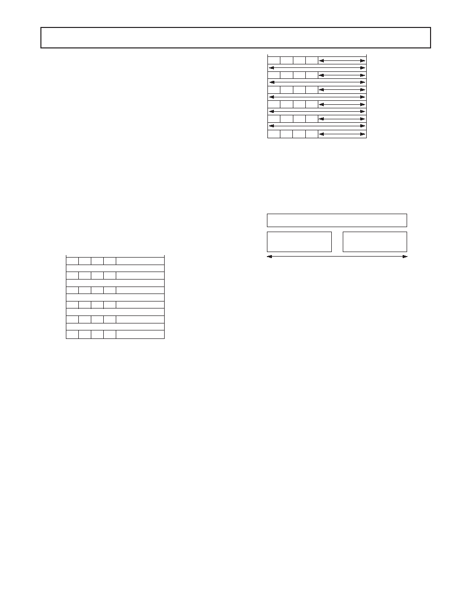
lowed by “1111” into the next channel selection field. Figure 11
shows a typical preconfiguration of external memory.
11
00
11
00
11
10
0
01
0
1
00
10
00000AH
000000H
STOP COMMAND
REPEAT LAST CHANNEL
FOR A VALID STOP
CONDITION
CONVERT ADC CH#3
CONVERT TEMP SENSOR
CONVERT ADC CH#5
CONVERT ADC CH#2
Figure 11. Typical DMA External Memory Preconfiguration
4. The DMA is initiated by writing to the ADC SFRs in the
following sequence.
a. ADCCON2 is written to enable the DMA mode, i.e.,
MOV ADCCON2, #40H; DMA mode enabled.
b. ADCCON1 is written to configure the conversion time and
power-up of the ADC. It can also enable Timer 2 driven
conversions or External Triggered conversions if required.
c. ADC conversions are initiated by starting single/continuous
conversions, starting Timer 2 running for Timer 2 conver-
sions, or by receiving an external trigger.
When the DMA conversions are completed, the ADC interrupt
bit ADCI is set by hardware and the external SRAM contains the
new ADC conversion results as shown in Figure 12. It should be
noted that no result is written to the last two memory locations.
When the DMA mode logic is active, it is responsible for storing
the ADC results away from both the user and ADuC812 core
logic. As it writes the results of the ADC conversions to external
memory, it takes over the external memory interface from the core.
Thus, any core instructions that access the external memory
while DMA mode is enabled will not gain access to it. The core
will execute the instructions and they will take the same time to
execute, but they will not gain access to the external memory.
NO CONVERSION
RESULT WRITTEN HERE
CONVERSION RESULT
FOR ADC CH#3
CONVERSION RESULT
FOR TEMP SENSOR
CONVERSION RESULT
FOR ADC CH#5
CONVERSION RESULT
FOR ADC CH#2
11
00
11
00
11
10
0
01
0
1
00
10
00000AH
000000H
STOP COMMAND
Figure 12. Typical External Memory Configuration Post
ADC DMA Operation
The DMA logic operates from the ADC clock and uses pipelining
to perform the ADC conversions and access the external memory
at the same time. The time it takes to perform one ADC conver-
sion is called a DMA cycle. The actions performed by the logic
during a typical DMA cycle are shown in Figure 13.
WRITE ADC RESULT
CONVERTED DURING
PREVIOUS DMA CYCLE
READ CHANNEL ID
TO BE CONVERTED DURING
NEXT DMA CYCLE
CONVERT CHANNEL READ DURING PREVIOUS DMA CYCLE
DMA CYCLE
Figure 13. DMA Cycle
From the previous diagram, it can be seen that during one DMA
cycle the following actions are performed by the DMA logic.
1. An ADC conversion is performed on the channel whose ID
was read during the previous cycle.
2. The 12-bit result and the channel ID of the conversion per-
formed in the previous cycle are written to the external memory.
3. The ID of the next channel to be converted is read from
external memory.
For the previous example, the complete flow of events is shown
in Figure 13. Because the DMA logic uses pipelining, it takes
three cycles before the first correct result is written out.
Micro Operation during ADC DMA Mode
During ADC DMA mode, the MicroConverter core is free to
continue code execution, including general housekeeping and
communication tasks. However, it should be noted that MCU core
accesses to Ports 0 and 2 (which are being used by the DMA
controller) are gated OFF during ADC DMA mode of operation.
This means that even though the instruction that accesses the
external Ports 0 or 2 will appear to execute, no data will be seen
at these external ports as a result.
The MicroConverter core can be configured with an interrupt
to be triggered by the DMA controller when it has finished
filling the requested block of RAM with ADC results, allowing
the service routine for this interrupt to postprocess data without
any real-time timing constraints.
Offset and Gain Calibration Coefficients
The ADuC812 has two ADC calibration coefficients, one for offset
calibration and one for gain calibration. Both the offset and gain
calibration coefficients are 14-bit words, located in the Special
Function Register (SFR) area. The offset calibration coefficient
is divided into ADCOFSH (six bits) and ADCOFSL (eight bits),
F
相关PDF资料 |
PDF描述 |
|---|---|
| AT32UC3C1512C-AZT | IC MCU 32BIT 512KB FLASH 100TQFP |
| VI-JVP-IY-F3 | CONVERTER MOD DC/DC 13.8V 50W |
| VE-233-IY-F2 | CONVERTER MOD DC/DC 24V 50W |
| VE-233-IY-F1 | CONVERTER MOD DC/DC 24V 50W |
| VE-2NY-IW-F1 | CONVERTER MOD DC/DC 3.3V 66W |
相关代理商/技术参数 |
参数描述 |
|---|---|
| ADUC812BSZ-01 | 制造商:Analog Devices 功能描述:12-BIT ADC WITH EMBEDDED MCU I.C. |
| ADUC812BSZ-REEL | 功能描述:IC MCU FLASH 12BIT ADC 52MQFP RoHS:是 类别:集成电路 (IC) >> 嵌入式 - 微控制器, 系列:MicroConverter® ADuC8xx 标准包装:38 系列:Encore!® XP® 核心处理器:eZ8 芯体尺寸:8-位 速度:5MHz 连通性:IrDA,UART/USART 外围设备:欠压检测/复位,LED,POR,PWM,WDT 输入/输出数:16 程序存储器容量:4KB(4K x 8) 程序存储器类型:闪存 EEPROM 大小:- RAM 容量:1K x 8 电压 - 电源 (Vcc/Vdd):2.7 V ~ 3.6 V 数据转换器:- 振荡器型:内部 工作温度:-40°C ~ 105°C 封装/外壳:20-SOIC(0.295",7.50mm 宽) 包装:管件 其它名称:269-4116Z8F0413SH005EG-ND |
| ADUC813BS | 制造商:Analog Devices 功能描述:12-BIT ADC WITH EMBEDDED MCU I.C. - Trays |
| ADUC814 | 制造商:AD 制造商全称:Analog Devices 功能描述:MicroConverter, Small Package 12-Bit ADC with Embedded Flash MCU |
| ADUC814_02 | 制造商:AD 制造商全称:Analog Devices 功能描述:MicroConverter, Small Package 12-Bit ADC with Embedded FLASH MCU |
发布紧急采购,3分钟左右您将得到回复。