- 您现在的位置:买卖IC网 > PDF目录12014 > ADUC836BSZ (Analog Devices Inc)IC ADC DUAL 16BIT W/MCU 52-MQFP PDF资料下载
参数资料
| 型号: | ADUC836BSZ |
| 厂商: | Analog Devices Inc |
| 文件页数: | 18/80页 |
| 文件大小: | 0K |
| 描述: | IC ADC DUAL 16BIT W/MCU 52-MQFP |
| 产品培训模块: | Process Control |
| 标准包装: | 1 |
| 系列: | MicroConverter® ADuC8xx |
| 核心处理器: | 8052 |
| 芯体尺寸: | 8-位 |
| 速度: | 12.58MHz |
| 连通性: | EBI/EMI,I²C,SPI,UART/USART |
| 外围设备: | POR,PSM,PWM,温度传感器,WDT |
| 输入/输出数: | 34 |
| 程序存储器容量: | 62KB(62K x 8) |
| 程序存储器类型: | 闪存 |
| EEPROM 大小: | 4K x 8 |
| RAM 容量: | 2.25K x 8 |
| 电压 - 电源 (Vcc/Vdd): | 2.7 V ~ 5.25 V |
| 数据转换器: | A/D 7x16b; D/A 1x12b |
| 振荡器型: | 内部 |
| 工作温度: | -40°C ~ 125°C |
| 封装/外壳: | 52-QFP |
| 包装: | 托盘 |
| 产品目录页面: | 738 (CN2011-ZH PDF) |
第1页第2页第3页第4页第5页第6页第7页第8页第9页第10页第11页第12页第13页第14页第15页第16页第17页当前第18页第19页第20页第21页第22页第23页第24页第25页第26页第27页第28页第29页第30页第31页第32页第33页第34页第35页第36页第37页第38页第39页第40页第41页第42页第43页第44页第45页第46页第47页第48页第49页第50页第51页第52页第53页第54页第55页第56页第57页第58页第59页第60页第61页第62页第63页第64页第65页第66页第67页第68页第69页第70页第71页第72页第73页第74页第75页第76页第77页第78页第79页第80页
ADuC836
–24–
ADuC836
–25–
Primary and Auxiliary ADC Inputs
The output of the Primary ADC multiplexer feeds into a high
impedance input stage of the buffer amplifier. As a result, the
primary ADC inputs can handle significant source impedances
and are tailored for direct connection to external resistive-type sen-
sors like strain gages or Resistance Temperature Detectors (RTDs).
The auxiliary ADC, however, is unbuffered, resulting in higher
analog input current on the auxiliary ADC. It should be noted
that this unbuffered input path provides a dynamic load to the
driving source.Therefore, resistor/capacitor combinations on the
input pins can cause dc gain errors depending on the output
impedance of the source that is driving the ADC inputs.
Analog Input Ranges
The absolute input voltage range on the primary ADC is restricted
to between AGND + 100 mV to AVDD – 100 mV. Care must be
taken in setting up the common-mode voltage and input voltage
range so that these limits are not exceeded; otherwise there will
be a degradation in linearity performance.
The absolute input voltage range on the auxiliary ADC is restricted
to between AGND – 30 mV to AVDD + 30 mV.The slightly negative
absolute input voltage limit does allow the possibility of monitor-
ing small signal bipolar signals using the single-ended auxiliary
ADC front end.
Programmable Gain Amplifier
The output from the buffer on the primary ADC is applied to the
input of the on-chip programmable gain amplifier (PGA).The
PGA can be programmed through eight different unipolar input
ranges and bipolar ranges.The PGA gain range is programmed
via the range bits in the ADC0CON SFR.With the external
reference select bit set in the ADC0CON SFR and an external
2.5 V reference, the unipolar ranges are 0 mV to 20 mV, 0 mV to
40 mV, 0 mV to 80 mV, 0 mV to 160 mV, 0 mV to 320 mV, 0 mV
to 640 mV, 0 V to 1.28 V, and 0 to 2.56 V; the bipolar ranges
are ±20 mV, ±40 mV, ±80 mV, ±160 mV, ±320 mV, ±640 mV,
±1.28 V, and ±2.56 V.These are the nominal ranges that should
appear at the input to the on-chip PGA. An ADC range matching
specification of 2 V (typ) across all ranges means that calibration
need only be carried out at a single gain range and does not have
to be repeated when the PGA gain range is changed.
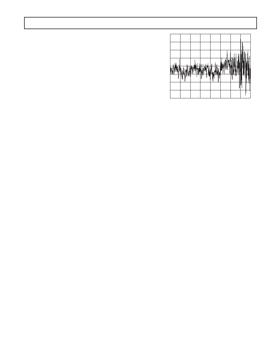
Typical matching across ranges is shown in Figure 9. Here, the
primary ADC is configured in bipolar mode with an external 2.5 V
reference, while just greater than 19 mV is forced on its inputs.
The ADC continuously converts the dc input voltage at an update
rate of 5.35 Hz, i.e., SF = FFH. In total, 800 conversion results are
gathered.The first 100 results are gathered with the primary ADC
operating in the ±20 mV range.The ADC range is then switched
to ±40 mV, 100 more conversion results are gathered, and so on,
until the last group of 100 samples is gathered with the ADC con-
figured in the ±2.56 V range. From Figure 9, the variation in the
sample mean through each range, i.e., the range matching, is seen
to be of the order of 2 V.
The auxiliary ADC does not incorporate a PGA and is configured
for a fixed single input range of 0 to VREF.
0
100
200
300
400
500
600
700
800
SAMPLE COUNT
ADC
INPUT
VOLTAGE
–
mV
19.372
19.371
19.370
19.369
19.368
19.367
19.366
19.365
19.364
ADC RANGE
20m
V
40m
V
80m
V
320m
V
2.56V
160m
V
640m
V
1.28V
Figure 9. Primary ADC Range Matching
Bipolar/Unipolar Inputs
The analog inputs on the ADuC836 can accept either unipolar
or bipolar input voltage ranges. Bipolar input ranges do not imply
that the part can handle negative voltages with respect to system
AGND.
Unipolar and bipolar signals on the AIN(+) input on the primary
ADC are referenced to the voltage on the respective AIN(–)
input. For example, if AIN(–) is 2.5 V and the primary ADC is
configured for an analog input range of 0 mV to 20 mV, the input
voltage range on the AIN(+) input is 2.5 V to 2.52 V. If AIN(–) is
2.5 V and the ADuC836 is configured for an analog input range
of 1.28 V, the analog input range on the AIN(+) input is 1.22 V to
3.78 V (i.e., 2.5 V ± 1.28 V).
As mentioned earlier, the auxiliary ADC input is a single-ended
input with respect to the system AGND. In this context, a bipolar
signal on the auxiliary ADC can only span 30 mV negative with
respect to AGND before violating the voltage input limits for
this ADC.
Bipolar or unipolar options are chosen by programming the pri-
mary and auxiliary Unipolar enable bits in the ADC0CON and
ADC1CON SFRs, respectively.This programs the relevant ADC
for either unipolar or bipolar operation. Programming for either
unipolar or bipolar operation does not change any of the input
signal conditioning; it simply changes the data output coding
and the points on the transfer function where calibrations occur.
When an ADC is configured for unipolar operation, the output
coding is natural (straight) binary with a zero differential input
voltage resulting in a code of 000 . . . 000, a midscale voltage
resulting in a code of 100 . . . 000, and a full-scale input voltage
resulting in a code of 111 . . . 111.When an ADC is configured
for bipolar operation, the coding is offset binary with a negative
full-scale voltage resulting in a code of 000 . . . 000, a zero dif-
ferential voltage resulting in a code of 100 . . . 000, and a positive
full-scale voltage resulting in a code of 111 . . . 111.
REV. A
相关PDF资料 |
PDF描述 |
|---|---|
| ADUC841BSZ62-5 | IC ADC/DAC 12BIT W/MCU 52-MQFP |
| VJ1825Y103JBGAT4X | CAP CER 10000PF 1KV 5% X7R 1825 |
| SCRU-01 | CONN RCPT IP68 USB A PNL MNT |
| VJ1825Y153JBGAT4X | CAP CER 0.015UF 1KV 5% X7R 1825 |
| VJ1825Y223JBGAT4X | CAP CER 0.022UF 1KV 5% X7R 1825 |
相关代理商/技术参数 |
参数描述 |
|---|---|
| ADUC841 | 制造商:AD 制造商全称:Analog Devices 功能描述:MicroConverter 12-Bit ADCs and DACs with Embedded High Speed 62-kB Flash MCU |
| ADUC841BCP32-5 | 制造商:Analog Devices 功能描述:MICROCONVERTER 1-CYCLE VERSION ADUC829 - Trays |
| ADUC841BCP62-3 | 制造商:Analog Devices 功能描述:MCU 8-Bit ADuC8xx 8052 CISC 62KB Flash 3V 56-Pin LFCSP EP 制造商:Rochester Electronics LLC 功能描述:8BIT CISC 62KB FLASH 20MHZ 3.3V 56LFCSP - Bulk |
| ADUC841BCP62-5 | 制造商:Analog Devices 功能描述:MCU 8-Bit ADuC8xx 8052 CISC 62KB Flash 5V 56-Pin LFCSP EP |
| ADUC841BCP8-3 | 制造商:Analog Devices 功能描述:MCU 8-bit ADuC8xx 8052 CISC 62KB Flash 3V 56-Pin LFCSP EP 制造商:Rochester Electronics LLC 功能描述:8BIT CISC 62KB FLASH 20MHZ 3.3V 56LFCSP - Bulk |
发布紧急采购,3分钟左右您将得到回复。