参数资料
| 型号: | ADV7180WBCPZ |
| 厂商: | Analog Devices Inc |
| 文件页数: | 22/116页 |
| 文件大小: | 0K |
| 描述: | IC VIDEO DECODER SDTV 40LFCSP |
| 标准包装: | 1 |
| 类型: | 视频解码器 |
| 应用: | 数码相机,手机,便携式视频 |
| 安装类型: | 表面贴装 |
| 封装/外壳: | 40-VFQFN 裸露焊盘,CSP |
| 供应商设备封装: | 40-LFCSP-VQ(6x6) |
| 包装: | 托盘 |
第1页第2页第3页第4页第5页第6页第7页第8页第9页第10页第11页第12页第13页第14页第15页第16页第17页第18页第19页第20页第21页当前第22页第23页第24页第25页第26页第27页第28页第29页第30页第31页第32页第33页第34页第35页第36页第37页第38页第39页第40页第41页第42页第43页第44页第45页第46页第47页第48页第49页第50页第51页第52页第53页第54页第55页第56页第57页第58页第59页第60页第61页第62页第63页第64页第65页第66页第67页第68页第69页第70页第71页第72页第73页第74页第75页第76页第77页第78页第79页第80页第81页第82页第83页第84页第85页第86页第87页第88页第89页第90页第91页第92页第93页第94页第95页第96页第97页第98页第99页第100页第101页第102页第103页第104页第105页第106页第107页第108页第109页第110页第111页第112页第113页第114页第115页第116页
Data Sheet
ADV7180
Rev. I | Page 13 of 116
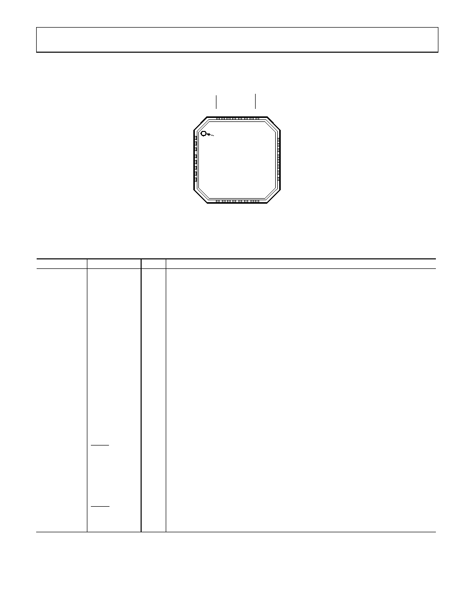
PIN CONFIGURATIONS AND FUNCTION DESCRIPTIONS
32-LEAD LFCSP
05
70
0-
0
57
NOTES
1. THE EXPOSEDPAD MUST BE CONNECTEDTO GND.
1
2
3
4
5
6
7
8
HS
DGND
DVDDIO
SFL
P7
P6
P5
P4
17
18
19
20
21
22
23
24
ELPF
PVDD
AIN1
VREFP
VREFN
AVDD
AIN2
AIN3
PIN1
INDICATOR
ADV7180
LFCSP
TOP VIEW
(Not to Scale)
25
26
27
28
29
30
31
32
16
15
14
13
12
11
10
9
P0
P1
DV
DD
XT
A
L
XT
A
L
1
LL
C
P2
P3
R
ESE
T
AL
S
B
S
DAT
A
SC
L
K
DG
ND
DV
DD
VS/
F
IE
L
D
IN
TR
Q
Figure 8. 32-Lead LFCSP Pin Configuration
Table 9. 32-Lead LFCSP Pin Function Descriptions
Pin No.
Mnemonic
Type
Description
1
HS
O
Horizontal Synchronization Output Signal.
2, 29
DGND
G
Ground for Digital Supply.
3
DVDDIO
P
Digital I/O Supply Voltage (1.8 V to 3.3 V).
4
SFL
O
Subcarrier Frequency Lock. This pin contains a serial output stream that can be used to lock the
subcarrier frequency when this decoder is connected to any Analog Devices digital video encoder.
5 to 10, 15, 16
P7 to P2, P1, P0
O
Video Pixel Output Port.
11
LLC
O
Line-Locked Output Clock for the Output Pixel Data. Nominally 27 MHz but varies up or
down according to video line length.
12
XTAL1
O
This pin should be connected to the 28.6363 MHz crystal or not connected if an external
1.8 V, 28.6363 MHz clock oscillator source is used to clock the ADV7180. In crystal mode, the
crystal must be a fundamental crystal.
13
XTAL
I
Input Pin for the 28.6363 MHz Crystal. This pin can be overdriven by an external 1.8 V,
28.6363 MHz clock oscillator source. In crystal mode, the crystal must be a fundamental crystal.
14, 30
DVDD
P
Digital Supply Voltage (1.8 V).
17
ELPF
I
The recommended external loop filter must be connected to this ELPF pin, as shown in Figure 60.
18
PVDD
P
PLL Supply Voltage (1.8 V).
19, 23, 24
AIN1 to AIN3
I
Analog Video Input Channels.
20
VREFP
O
Internal Voltage Reference Output. See Figure 60 for recommended output circuitry.
21
VREFN
O
Internal Voltage Reference Output. See Figure 60 for recommended output circuitry.
22
AVDD
P
Analog Supply Voltage (1.8 V).
25
RESET
I
System Reset Input. Active low. A minimum low reset pulse width of 5 ms is required to
reset the ADV7180 circuitry.
26
ALSB
I
for a write is Address 0x40; for ALSB set to Logic 1, the address selected is Address 0x42.
27
SDATA
I/O
I2C Port Serial Data Input/Output Pin.
28
SCLK
I
I2C Port Serial Clock Input. The maximum clock rate is 400 kHz.
31
VS/FIELD
O
Vertical Synchronization Output Signal/Field Synchronization Output Signal.
32
INTRQ
O
Interrupt Request Output. Interrupt occurs when certain signals are detected on the input video
EPAD (EP)
The exposed pad must be connected to GND.
相关PDF资料 |
PDF描述 |
|---|---|
| ADV7186BBCZ | IC VIDEO DECODER 196CSPBGA |
| ADV7441ABSTZ-5P | IC DECODER DIGITIZER 144LQFP |
| ADV7513BSWZ | IC TX HDMI 165MHZ 64LQFP |
| ADV7520BCPZ-80 | IC XMITTER HDMI/DVI CEC 64LFCSP |
| ADV7520NKBBCZ-80 | IC XMITTER HDMI/DVI LP 76CSPBGA |
相关代理商/技术参数 |
参数描述 |
|---|---|
| ADV7180WBCPZ-REEL | 功能描述:IC VIDEO DECODER SDTV 40LFCSP RoHS:是 类别:集成电路 (IC) >> 线性 - 视频处理 系列:- 产品变化通告:Product Discontinuation 07/Mar/2011 标准包装:3,000 系列:OMNITUNE™ 类型:调谐器 应用:移动电话,手机,视频显示器 安装类型:表面贴装 封装/外壳:65-WFBGA 供应商设备封装:PG-WFSGA-65 包装:带卷 (TR) 其它名称:SP000365064 |
| ADV7180WBST48Z | 制造商:Analog Devices 功能描述: |
| ADV7180WBST48Z-RL | 功能描述:视频 IC 10-bit 4x Oversampling SDTV Decoder RoHS:否 制造商:Fairchild Semiconductor 工作电源电压:5 V 电源电流:80 mA 最大工作温度:+ 85 C 封装 / 箱体:TSSOP-28 封装:Reel |
| ADV7180WBSTZ | 功能描述:视频 IC 10-bit 4x Oversampling SDTV Decoder RoHS:否 制造商:Fairchild Semiconductor 工作电源电压:5 V 电源电流:80 mA 最大工作温度:+ 85 C 封装 / 箱体:TSSOP-28 封装:Reel |
| ADV7180WBSTZ-REEL | 功能描述:视频 IC 10-bit 4x Oversampling SDTV Decoder RoHS:否 制造商:Fairchild Semiconductor 工作电源电压:5 V 电源电流:80 mA 最大工作温度:+ 85 C 封装 / 箱体:TSSOP-28 封装:Reel |
发布紧急采购,3分钟左右您将得到回复。