- 您现在的位置:买卖IC网 > PDF目录17033 > AFS-EVAL-KIT (Microsemi SoC)KIT STARTER EVAL FUSION AFS600 PDF资料下载
参数资料
| 型号: | AFS-EVAL-KIT |
| 厂商: | Microsemi SoC |
| 文件页数: | 87/334页 |
| 文件大小: | 0K |
| 描述: | KIT STARTER EVAL FUSION AFS600 |
| 标准包装: | 1 |
| 系列: | Fusion® |
| 类型: | FPGA |
| 适用于相关产品: | AFS600-FG256 |
| 所含物品: | 板,DVD,电源,编程器 |
| 其它名称: | 1100-1148 |
第1页第2页第3页第4页第5页第6页第7页第8页第9页第10页第11页第12页第13页第14页第15页第16页第17页第18页第19页第20页第21页第22页第23页第24页第25页第26页第27页第28页第29页第30页第31页第32页第33页第34页第35页第36页第37页第38页第39页第40页第41页第42页第43页第44页第45页第46页第47页第48页第49页第50页第51页第52页第53页第54页第55页第56页第57页第58页第59页第60页第61页第62页第63页第64页第65页第66页第67页第68页第69页第70页第71页第72页第73页第74页第75页第76页第77页第78页第79页第80页第81页第82页第83页第84页第85页第86页当前第87页第88页第89页第90页第91页第92页第93页第94页第95页第96页第97页第98页第99页第100页第101页第102页第103页第104页第105页第106页第107页第108页第109页第110页第111页第112页第113页第114页第115页第116页第117页第118页第119页第120页第121页第122页第123页第124页第125页第126页第127页第128页第129页第130页第131页第132页第133页第134页第135页第136页第137页第138页第139页第140页第141页第142页第143页第144页第145页第146页第147页第148页第149页第150页第151页第152页第153页第154页第155页第156页第157页第158页第159页第160页第161页第162页第163页第164页第165页第166页第167页第168页第169页第170页第171页第172页第173页第174页第175页第176页第177页第178页第179页第180页第181页第182页第183页第184页第185页第186页第187页第188页第189页第190页第191页第192页第193页第194页第195页第196页第197页第198页第199页第200页第201页第202页第203页第204页第205页第206页第207页第208页第209页第210页第211页第212页第213页第214页第215页第216页第217页第218页第219页第220页第221页第222页第223页第224页第225页第226页第227页第228页第229页第230页第231页第232页第233页第234页第235页第236页第237页第238页第239页第240页第241页第242页第243页第244页第245页第246页第247页第248页第249页第250页第251页第252页第253页第254页第255页第256页第257页第258页第259页第260页第261页第262页第263页第264页第265页第266页第267页第268页第269页第270页第271页第272页第273页第274页第275页第276页第277页第278页第279页第280页第281页第282页第283页第284页第285页第286页第287页第288页第289页第290页第291页第292页第293页第294页第295页第296页第297页第298页第299页第300页第301页第302页第303页第304页第305页第306页第307页第308页第309页第310页第311页第312页第313页第314页第315页第316页第317页第318页第319页第320页第321页第322页第323页第324页第325页第326页第327页第328页第329页第330页第331页第332页第333页第334页
Fusion Family of Mixed Signal FPGAs
Revision 4
2-161
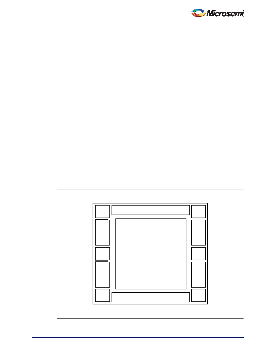
User I/O Naming Convention
Due to the comprehensive and flexible nature of Fusion device user I/Os, a naming scheme is used to
show the details of the I/O (Figure 2-113 on page 2-161 and Figure 2-114 on page 2-162). The name
identifies to which I/O bank it belongs, as well as the pairing and pin polarity for differential I/Os.
I/O Nomenclature
= Gmn/IOuxwByVz
Gmn is only used for I/Os that also have CCC access—i.e., global pins.
G
= Global
m
= Global pin location associated with each CCC on the device: A (northwest corner), B (northeast corner), C
(east middle), D (southeast corner), E (southwest corner), and F (west middle).
n
= Global input MUX and pin number of the associated Global location m, either A0, A1, A2, B0, B1, B2, C0, C1,
or C2. Figure 2-22 on page 2-27 shows the three input pins per clock source MUX at CCC location m.
u
= I/O pair number in the bank, starting at 00 from the northwest I/O bank and proceeding in a clockwise
direction.
x
= P (Positive) or N (Negative) for differential pairs, or R (Regular – single-ended) for the I/Os that support single-
ended and voltage-referenced I/O standards only. U (Positive-LVDS only) or V (Negative-LVDS only) restrict
the I/O differential pair from being selected as an LVPECL pair.
w
= D (Differential Pair), P (Pair), or S (Single-Ended). D (Differential Pair) if both members of the pair are bonded
out to adjacent pins or are separated only by one GND or NC pin; P (Pair) if both members of the pair are
bonded out but do not meet the adjacency requirement; or S (Single-Ended) if the I/O pair is not bonded out.
For Differential (D) pairs, adjacency for ball grid packages means only vertical or horizontal. Diagonal
adjacency does not meet the requirements for a true differential pair.
B
= Bank
y
= Bank number (0–3). The Bank number starts at 0 from the northwest I/O bank and proceeds in a clockwise
direction.
V
= Reference voltage
z
= Minibank number
Figure 2-113 Naming Conventions of Fusion Devices with Three Digital I/O Banks
CCC
"A"
CCC
"E"
CCC/PLL
"F"
CCC
"B"
CCC
"D"
CCC
"C"
AFS090
Standard I/O Bank
Analog Quads
Advanced
I/O
Bank
Advanced
I/O
Bank
AFS250
Bank 3
Bank 1
Bank 2 (analog)
Bank 0
相关PDF资料 |
PDF描述 |
|---|---|
| ESM10DRYS | CONN EDGECARD 20POS DIP .156 SLD |
| EMM11DRTN | CONN EDGECARD 22POS DIP .156 SLD |
| AGL-ICICLE-KIT | KIT EVAL FOR IGOO ICICLE |
| ECM25DCCN | CONN EDGECARD 50POS R/A .156 SLD |
| DC1266A-A | BOARD DELTA SIGMA ADC LTC2453 |
相关代理商/技术参数 |
参数描述 |
|---|---|
| AFSIMG-4735101M-NP | 制造商:Sumida Corporation 功能描述:Inductor (no Datasheet to get info) 制造商:SUMIDA ELECTRONICS 功能描述:Inductor (no Datasheet to get info) |
| AFSK-12A-70 | 制造商:MACOM 制造商全称:Tyco Electronics 功能描述:FLEXSRRIP PIN CONFIGURATIONS, GENERIC |
| AFSK-12B-70 | 制造商:MACOM 制造商全称:Tyco Electronics 功能描述:FLEXSRRIP PIN CONFIGURATIONS, GENERIC |
| AFSK-12C-70 | 制造商:MACOM 制造商全称:Tyco Electronics 功能描述:FLEXSRRIP PIN CONFIGURATIONS, GENERIC |
| AFSK-12D-70 | 制造商:MACOM 制造商全称:Tyco Electronics 功能描述:FLEXSRRIP PIN CONFIGURATIONS, GENERIC |
发布紧急采购,3分钟左右您将得到回复。