- 您现在的位置:买卖IC网 > PDF目录17033 > AFS-EVAL-KIT (Microsemi SoC)KIT STARTER EVAL FUSION AFS600 PDF资料下载
参数资料
| 型号: | AFS-EVAL-KIT |
| 厂商: | Microsemi SoC |
| 文件页数: | 98/334页 |
| 文件大小: | 0K |
| 描述: | KIT STARTER EVAL FUSION AFS600 |
| 标准包装: | 1 |
| 系列: | Fusion® |
| 类型: | FPGA |
| 适用于相关产品: | AFS600-FG256 |
| 所含物品: | 板,DVD,电源,编程器 |
| 其它名称: | 1100-1148 |
第1页第2页第3页第4页第5页第6页第7页第8页第9页第10页第11页第12页第13页第14页第15页第16页第17页第18页第19页第20页第21页第22页第23页第24页第25页第26页第27页第28页第29页第30页第31页第32页第33页第34页第35页第36页第37页第38页第39页第40页第41页第42页第43页第44页第45页第46页第47页第48页第49页第50页第51页第52页第53页第54页第55页第56页第57页第58页第59页第60页第61页第62页第63页第64页第65页第66页第67页第68页第69页第70页第71页第72页第73页第74页第75页第76页第77页第78页第79页第80页第81页第82页第83页第84页第85页第86页第87页第88页第89页第90页第91页第92页第93页第94页第95页第96页第97页当前第98页第99页第100页第101页第102页第103页第104页第105页第106页第107页第108页第109页第110页第111页第112页第113页第114页第115页第116页第117页第118页第119页第120页第121页第122页第123页第124页第125页第126页第127页第128页第129页第130页第131页第132页第133页第134页第135页第136页第137页第138页第139页第140页第141页第142页第143页第144页第145页第146页第147页第148页第149页第150页第151页第152页第153页第154页第155页第156页第157页第158页第159页第160页第161页第162页第163页第164页第165页第166页第167页第168页第169页第170页第171页第172页第173页第174页第175页第176页第177页第178页第179页第180页第181页第182页第183页第184页第185页第186页第187页第188页第189页第190页第191页第192页第193页第194页第195页第196页第197页第198页第199页第200页第201页第202页第203页第204页第205页第206页第207页第208页第209页第210页第211页第212页第213页第214页第215页第216页第217页第218页第219页第220页第221页第222页第223页第224页第225页第226页第227页第228页第229页第230页第231页第232页第233页第234页第235页第236页第237页第238页第239页第240页第241页第242页第243页第244页第245页第246页第247页第248页第249页第250页第251页第252页第253页第254页第255页第256页第257页第258页第259页第260页第261页第262页第263页第264页第265页第266页第267页第268页第269页第270页第271页第272页第273页第274页第275页第276页第277页第278页第279页第280页第281页第282页第283页第284页第285页第286页第287页第288页第289页第290页第291页第292页第293页第294页第295页第296页第297页第298页第299页第300页第301页第302页第303页第304页第305页第306页第307页第308页第309页第310页第311页第312页第313页第314页第315页第316页第317页第318页第319页第320页第321页第322页第323页第324页第325页第326页第327页第328页第329页第330页第331页第332页第333页第334页
Fusion Family of Mixed Signal FPGAs
Revision 4
2-171
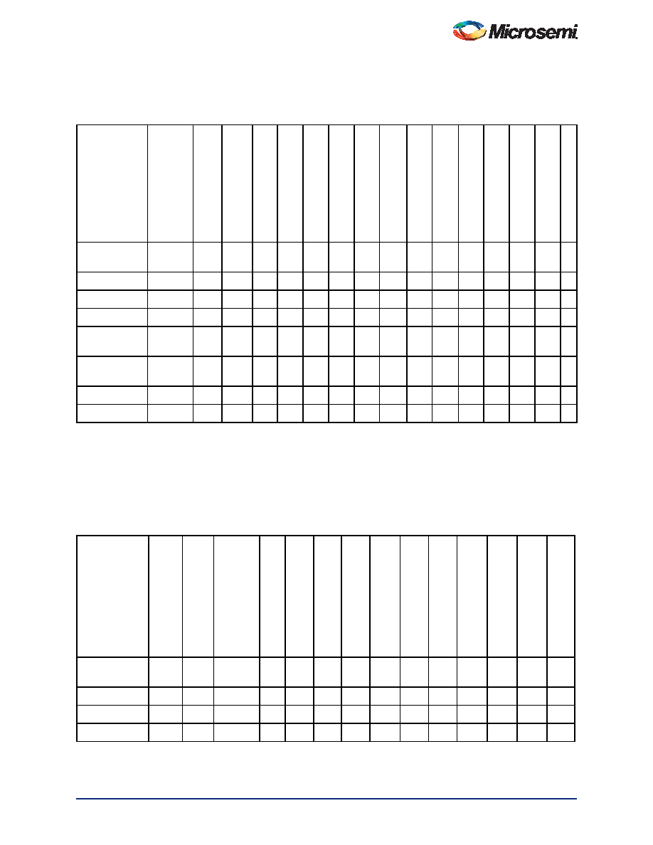
Table 2-93 Summary of I/O Timing Characteristics – Software Default Settings
Commercial Temperature Range Conditions: TJ = 70°C, Worst-Case VCC = 1.425 V,
Worst-Case VCCI = I/O Standard Dependent
Applicable to Advanced I/Os
I/O Standard
Drive
S
trength
(mA)
Slew
Rat
e
Ca
p
acitive
Lo
ad
(p
F)
External
Re
si
st
or
(O
hm)
t
DO
U
T
t
DP
t
DI
N
t
PY
t
EOUT
t
ZL
t
ZH
t
LZ
t
HZ
t
ZLS
t
ZH
S
Unit
s
3.3 V LVTTL/
3.3 V LVCMOS
12 mA
High 35 pF
–
0.49 2.64 0.03 0.90 0.32 2.69 2.11 2.40 2.68 4.36 3.78 ns
2.5 V LVCMOS
12 mA
High 35 pF
–
0.49 2.66 0.03 0.98 0.32 2.71 2.56 2.47 2.57 4.38 4.23 ns
1.8 V LVCMOS
12 mA
High 35 pF
–
0.49 2.64 0.03 0.91 0.32 2.69 2.27 2.76 3.05 4.36 3.94 ns
1.5 V LVCMOS
12 mA
High 35 pF
–
0.49 3.05 0.03 1.07 0.32 3.10 2.67 2.95 3.14 4.77 4.34 ns
3.3 V PCI
Per PCI
spec
High 10 pF 25 2 0.49 2.00 0.03 0.65 0.32 2.04 1.46 2.40 2.68 3.71 3.13 ns
3.3 V PCI-X
Per PCI-X
spec
High 10 pF 25 2 0.49 2.00 0.03 0.62 0.32 2.04 1.46 2.40 2.68 3.71 3.13 ns
LVDS
24 mA
High
–
0.49 1.37 0.03 1.20 N/A N/A N/A N/A N/A N/A N/A ns
LVPECL
24 mA
High
–
0.49 1.34 0.03 1.05 N/A N/A N/A N/A N/A N/A N/A ns
Notes:
1. For specific junction temperature and voltage-supply levels, refer to Table 3-6 on page 3-7 for derating values.
2. Resistance is used to measure I/O propagation delays as defined in PCI specifications. See Figure 2-123 on page 2-200
for connectivity. This resistor is not required during normal operation.
Table 2-94 Summary of I/O Timing Characteristics – Software Default Settings
Commercial Temperature Range Conditions: TJ = 70°C, Worst-Case VCC = 1.425 V,
Worst-Case VCCI = I/O Standard Dependent
Applicable to Standard I/Os
I/O Standard
Drive
S
trength
(mA)
Slew
Rate
Cap
acitiv
eLo
ad
(pF
)
Extern
al
Resisto
r(Oh
m
)
t
DO
U
T
t
DP
t
DI
N
t
PY
t
EOU
T
t
ZL
t
ZH
t
LZ
t
HZ
Unit
s
3.3 V LVTTL/
3.3 V LVCMOS
8 mA
High
35 pF
–
0.49 3.29 0.03 0.75 0.32 3.36 2.80
1.79
2.01
ns
2.5 V LVCMOS 8 mA
High
35pF
–
0.49 3.56 0.03 0.96 0.32 3.40 3.56
1.78
1.91
ns
1.8 V LVCMOS 4 mA
High
35pF
–
0.49 4.74 0.03 0.90 0.32 4.02 4.74
1.80
1.85
ns
1.5 V LVCMOS 2 mA
High
35pF
–
0.49 5.71 0.03 1.06 0.32 4.71 5.71
1.83
ns
Note: For specific junction temperature and voltage-supply levels, refer to Table 3-6 on page 3-7 for derating values.
相关PDF资料 |
PDF描述 |
|---|---|
| ESM10DRYS | CONN EDGECARD 20POS DIP .156 SLD |
| EMM11DRTN | CONN EDGECARD 22POS DIP .156 SLD |
| AGL-ICICLE-KIT | KIT EVAL FOR IGOO ICICLE |
| ECM25DCCN | CONN EDGECARD 50POS R/A .156 SLD |
| DC1266A-A | BOARD DELTA SIGMA ADC LTC2453 |
相关代理商/技术参数 |
参数描述 |
|---|---|
| AFSIMG-4735101M-NP | 制造商:Sumida Corporation 功能描述:Inductor (no Datasheet to get info) 制造商:SUMIDA ELECTRONICS 功能描述:Inductor (no Datasheet to get info) |
| AFSK-12A-70 | 制造商:MACOM 制造商全称:Tyco Electronics 功能描述:FLEXSRRIP PIN CONFIGURATIONS, GENERIC |
| AFSK-12B-70 | 制造商:MACOM 制造商全称:Tyco Electronics 功能描述:FLEXSRRIP PIN CONFIGURATIONS, GENERIC |
| AFSK-12C-70 | 制造商:MACOM 制造商全称:Tyco Electronics 功能描述:FLEXSRRIP PIN CONFIGURATIONS, GENERIC |
| AFSK-12D-70 | 制造商:MACOM 制造商全称:Tyco Electronics 功能描述:FLEXSRRIP PIN CONFIGURATIONS, GENERIC |
发布紧急采购,3分钟左右您将得到回复。