- 您现在的位置:买卖IC网 > Datasheet目录394 > AON2405 (Alpha & Omega Semiconductor Inc)MOSFET P CH 20V 8A DFN 2x2B Datasheet资料下载
参数资料
| 型号: | AON2405 |
| 厂商: | Alpha & Omega Semiconductor Inc |
| 文件页数: | 2/5页 |
| 文件大小: | 0K |
| 描述: | MOSFET P CH 20V 8A DFN 2x2B |
| 标准包装: | 1 |
| FET 型: | MOSFET P 通道,金属氧化物 |
| FET 特点: | 逻辑电平门 |
| 漏极至源极电压(Vdss): | 20V |
| 电流 - 连续漏极(Id) @ 25° C: | 8A |
| 开态Rds(最大)@ Id, Vgs @ 25° C: | 32 毫欧 @ 8A,4.5V |
| Id 时的 Vgs(th)(最大): | 900mV @ 250µA |
| 闸电荷(Qg) @ Vgs: | 18nC @ 4.5V |
| 输入电容 (Ciss) @ Vds: | 1025pF @ 10V |
| 功率 - 最大: | 2.8W |
| 安装类型: | 表面贴装 |
| 封装/外壳: | 6-UDFN 裸露焊盘 |
| 供应商设备封装: | 6-DFN-EP(2x2) |
| 包装: | 标准包装 |
| 其它名称: | 785-1392-6 |
�� �
�
�AON2405�
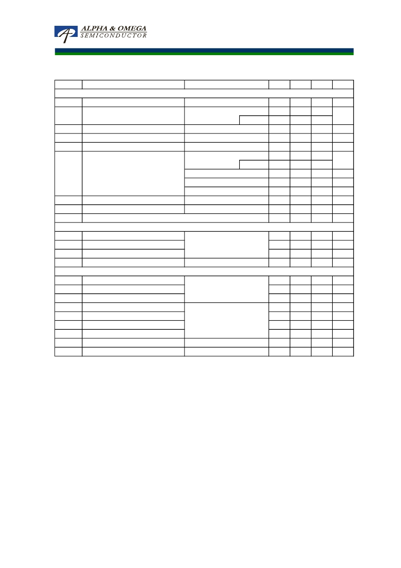
�Electrical� Characteristics� (T� J� =25°C� unless� otherwise� noted)�
�Symbol�
�Parameter�
�Conditions�
�Min�
�Typ�
�Max�
�Units�
�STATIC� PARAMETERS�
�BV� DSS�
�Drain-Source� Breakdown� Voltage�
�I� D� =-250� μ� A,� V� GS� =0V�
�-20�
�V�
�I� DSS�
�I� GSS�
�Zero� Gate� Voltage� Drain� Current�
�Gate-Body� leakage� current�
�V� DS� =-20V,� V� GS� =0V�
�V� DS� =0V,� V� GS� =±8V�
�T� J� =55°C�
�-1�
�-5�
�±100�
�μ� A�
�nA�
�V� GS(th)�
�I� D(ON)�
�R� DS(ON)�
�Gate� Threshold� Voltage�
�On� state� drain� current�
�Static� Drain-Source� On-Resistance�
�V� DS� =V� GS� ,� I� D� =-250� μ� A�
�V� GS� =-4.5V,� V� DS� =-5V�
�V� GS� =-4.5V,� I� D� =-8A�
�V� GS� =-2.5V,� I� D� =-5A�
�T� J� =125°C�
�-0.3�
�-32�
�-0.65�
�26�
�35�
�32�
�-0.9�
�32�
�43�
�41�
�V�
�A�
�m� ?�
�m� ?�
�V� GS� =-1.8V,� I� D� =-2A�
�V� GS� =-1.5V,� I� D� =-2A�
�41�
�46�
�56�
�70�
�m� ?�
�m� ?�
�g� FS�
�Forward� Transconductance�
�V� DS� =-5V,� I� D� =-8A�
�23�
�S�
�V� SD�
�Diode� Forward� Voltage�
�I� S� =-1A,V� GS� =0V�
�-0.62�
�-1�
�V�
�I� S�
�Maximum� Body-Diode� Continuous� Current�
�-4.5�
�A�
�DYNAMIC� PARAMETERS�
�C� iss�
�Input� Capacitance�
�1025�
�pF�
�C� oss�
�C� rss�
�R� g�
�Output� Capacitance�
�Reverse� Transfer� Capacitance�
�Gate� resistance�
�V� GS� =0V,� V� DS� =-10V,� f=1MHz�
�V� GS� =0V,� V� DS� =0V,� f=1MHz�
�167�
�119�
�11�
�pF�
�pF�
�?�
�SWITCHING� PARAMETERS�
�Q� g�
�Total� Gate� Charge�
�13�
�18�
�nC�
�Q� gs�
�Q� gd�
�t� D(on)�
�t� r�
�t� D(off)�
�t� f�
�t� rr�
�Gate� Source� Charge�
�Gate� Drain� Charge�
�Turn-On� DelayTime�
�Turn-On� Rise� Time�
�Turn-Off� DelayTime�
�Turn-Off� Fall� Time�
�Body� Diode� Reverse� Recovery� Time�
�V� GS� =-4.5V,� V� DS� =-10V,� I� D� =-8A�
�V� GS� =-4.5V,� V� DS� =-10V,�
�R� L� =1.25� ?� ,� R� GEN� =3� ?�
�I� F� =-8A,� dI/dt=100A/� μ� s�
�2�
�3.4�
�7�
�28�
�95�
�46�
�15�
�nC�
�nC�
�ns�
�ns�
�ns�
�ns�
�ns�
�Q� rr�
�Body� Diode� Reverse� Recovery� Charge� I� F� =-8A,� dI/dt=100A/� μ� s�
�4�
�nC�
�A.� The� value� of� R� θ� JA� is� measured� with� the� device� mounted� on� 1in� 2� FR-4� board� with� 2oz.� Copper,� in� a� still� air� environment� with� T� A� =25� °� C.� The�
�Power� dissipation� P� DSM� is� based� on� R� θ� JA� t� ≤� 10s� value� and� the� maximum� allowed� junction� temperature� of� 150� °� C.� The� value� in� any� given�
�application� depends� on� the� user's� specific� board� design.�
�B.� The� power� dissipation� P� D� is� based� on� T� J(MAX)� =150� °� C,� using� junction-to-case� thermal� resistance,� and� is� more� useful� in� setting� the� upper�
�dissipation� limit� for� cases� where� additional� heatsinking� is� used.�
�C.� Repetitive� rating,� pulse� width� limited� by� junction� temperature� T� J(MAX)� =150� °� C.� Ratings� are� based� on� low� frequency� and� duty� cycles� to� keep�
�initial� T� J� =25� °� C.�
�D.� The� R� θ� JA� is� the� sum� of� the� thermal� impedance� from� junction� to� case� R� θ� JC� and� case� to� ambient.�
�E.� The� static� characteristics� in� Figures� 1� to� 6� are� obtained� using� <300� μ� s� pulses,� duty� cycle� 0.5%� max.�
�F.� These� curves� are� based� on� the� junction-to-case� thermal� impedance� which� is� measured� with� the� device� mounted� to� a� large� heatsink,� assuming�
�a� maximum� junction� temperature� of� T� J(MAX)� =150� °� C.� The� SOA� curve� provides� a� single� pulse� rating.�
�G.� The� maximum� current� rating� is� package� limited.�
�H.� These� tests� are� performed� with� the� device� mounted� on� 1� in� 2� FR-4� board� with� 2oz.� Copper,� in� a� still� air� environment� with� T� A� =25� °� C.�
�THIS� PRODUCT� HAS� BEEN� DESIGNED� AND� QUALIFIED� FOR� THE� CONSUMER� MARKET.� APPLICATIONS� OR� USES� AS� CRITICAL�
�COMPONENTS� IN� LIFE� SUPPORT� DEVICES� OR� SYSTEMS� ARE� NOT� AUTHORIZED.� AOS� DOES� NOT� ASSUME� ANY� LIABILITY� ARISING�
�OUT� OF� SUCH� APPLICATIONS� OR� USES� OF� ITS� PRODUCTS.� AOS� RESERVES� THE� RIGHT� TO� IMPROVE� PRODUCT� DESIGN,�
�FUNCTIONS� AND� RELIABILITY� WITHOUT� NOTICE.�
�Rev� 2� :� Sep.� 2012�
�www.aosmd.com�
�Page� 2� of� 5�
�相关PDF资料 |
PDF描述 |
|---|---|
| AON6232 | MOSFET N CH 40V 85A DFN5X6 |
| AON6244 | MOSFET N CH 60V 85A DFN5X6 |
| AON6918 | MOSF 2N CH 25V 60/85A DFN5X6A |
| AON7421 | MOSF P CH 20V 50A DFN3.3X3.3EP |
| AON7423 | MOSF P CH 20V 50A DFN3.3X3.3EP |
相关代理商/技术参数 |
参数描述 |
|---|---|
| AON2406 | 制造商:Alpha & Omega Semiconductor 功能描述:Trans MOSFET N-CH 20V 8A 6-Pin DFN EP T/R 制造商:Alpha & Omega Semiconductor 功能描述:MOSFET N-CH 20V 8A 6LDFN |
| AON2407 | 功能描述:MOSFET P CH 30V 6.3A DFN 2x2B RoHS:是 类别:分离式半导体产品 >> FET - 单 系列:- 标准包装:1,000 系列:MESH OVERLAY™ FET 型:MOSFET N 通道,金属氧化物 FET 特点:逻辑电平门 漏极至源极电压(Vdss):200V 电流 - 连续漏极(Id) @ 25° C:18A 开态Rds(最大)@ Id, Vgs @ 25° C:180 毫欧 @ 9A,10V Id 时的 Vgs(th)(最大):4V @ 250µA 闸电荷(Qg) @ Vgs:72nC @ 10V 输入电容 (Ciss) @ Vds:1560pF @ 25V 功率 - 最大:40W 安装类型:通孔 封装/外壳:TO-220-3 整包 供应商设备封装:TO-220FP 包装:管件 |
| AON2408 | 功能描述:MOSFET N CH 20V 8A DFN 2x2B RoHS:是 类别:分离式半导体产品 >> FET - 单 系列:- 标准包装:1,000 系列:MESH OVERLAY™ FET 型:MOSFET N 通道,金属氧化物 FET 特点:逻辑电平门 漏极至源极电压(Vdss):200V 电流 - 连续漏极(Id) @ 25° C:18A 开态Rds(最大)@ Id, Vgs @ 25° C:180 毫欧 @ 9A,10V Id 时的 Vgs(th)(最大):4V @ 250µA 闸电荷(Qg) @ Vgs:72nC @ 10V 输入电容 (Ciss) @ Vds:1560pF @ 25V 功率 - 最大:40W 安装类型:通孔 封装/外壳:TO-220-3 整包 供应商设备封装:TO-220FP 包装:管件 |
| AON2409 | 功能描述:MOSFET P CH 30V 8A DFN 2x2B RoHS:是 类别:分离式半导体产品 >> FET - 单 系列:- 标准包装:1,000 系列:MESH OVERLAY™ FET 型:MOSFET N 通道,金属氧化物 FET 特点:逻辑电平门 漏极至源极电压(Vdss):200V 电流 - 连续漏极(Id) @ 25° C:18A 开态Rds(最大)@ Id, Vgs @ 25° C:180 毫欧 @ 9A,10V Id 时的 Vgs(th)(最大):4V @ 250µA 闸电荷(Qg) @ Vgs:72nC @ 10V 输入电容 (Ciss) @ Vds:1560pF @ 25V 功率 - 最大:40W 安装类型:通孔 封装/外壳:TO-220-3 整包 供应商设备封装:TO-220FP 包装:管件 |
| AON2410 | 功能描述:MOSFET N CH 30V 8A DFN 2x2B RoHS:是 类别:分离式半导体产品 >> FET - 单 系列:- 标准包装:1,000 系列:MESH OVERLAY™ FET 型:MOSFET N 通道,金属氧化物 FET 特点:逻辑电平门 漏极至源极电压(Vdss):200V 电流 - 连续漏极(Id) @ 25° C:18A 开态Rds(最大)@ Id, Vgs @ 25° C:180 毫欧 @ 9A,10V Id 时的 Vgs(th)(最大):4V @ 250µA 闸电荷(Qg) @ Vgs:72nC @ 10V 输入电容 (Ciss) @ Vds:1560pF @ 25V 功率 - 最大:40W 安装类型:通孔 封装/外壳:TO-220-3 整包 供应商设备封装:TO-220FP 包装:管件 |
发布紧急采购,3分钟左右您将得到回复。