- 您现在的位置:买卖IC网 > PDF目录11722 > AT89LP51-20PU (Atmel)MCU 8051 4K FLASH 20MHZ PDF资料下载
参数资料
| 型号: | AT89LP51-20PU |
| 厂商: | Atmel |
| 文件页数: | 29/117页 |
| 文件大小: | 0K |
| 描述: | MCU 8051 4K FLASH 20MHZ |
| 标准包装: | 10 |
| 系列: | 89LP |
| 核心处理器: | 8051 |
| 芯体尺寸: | 8-位 |
| 速度: | 20MHz |
| 连通性: | EBI/EMI,I²C,SPI,UART/USART |
| 外围设备: | 欠压检测/复位,POR,PWM,WDT |
| 输入/输出数: | 36 |
| 程序存储器容量: | 4KB(4K x 8) |
| 程序存储器类型: | 闪存 |
| RAM 容量: | 256 x 8 |
| 电压 - 电源 (Vcc/Vdd): | 2.4 V ~ 5.5 V |
| 振荡器型: | 内部 |
| 工作温度: | -40°C ~ 85°C |
| 封装/外壳: | 40-DIP(0.600",15.24mm) |
| 包装: | 管件 |
第1页第2页第3页第4页第5页第6页第7页第8页第9页第10页第11页第12页第13页第14页第15页第16页第17页第18页第19页第20页第21页第22页第23页第24页第25页第26页第27页第28页当前第29页第30页第31页第32页第33页第34页第35页第36页第37页第38页第39页第40页第41页第42页第43页第44页第45页第46页第47页第48页第49页第50页第51页第52页第53页第54页第55页第56页第57页第58页第59页第60页第61页第62页第63页第64页第65页第66页第67页第68页第69页第70页第71页第72页第73页第74页第75页第76页第77页第78页第79页第80页第81页第82页第83页第84页第85页第86页第87页第88页第89页第90页第91页第92页第93页第94页第95页第96页第97页第98页第99页第100页第101页第102页第103页第104页第105页第106页第107页第108页第109页第110页第111页第112页第113页第114页第115页第116页第117页
19
3709D–MICRO–12/11
AT89LP51/52
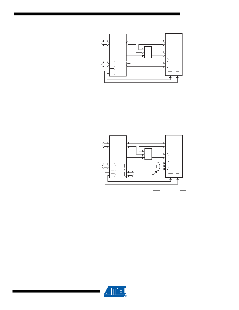
Figure 3-10. External Data Memory 16-bit Linear Address Mode
Figure 3-11 shows a hardware configuration for accessing 256-byte blocks of external RAM
using an 8-bit paged address. Port 0 serves as a multiplexed address/data bus to the RAM. The
ALE strobe is used to latch the address byte into an external register so that Port 0 can be freed
for data input/output. The Port 2 I/O lines (or other ports) can provide control lines to page the
memory; however, this operation is not handled automatically by hardware. The software appli-
cation must change the Port 2 register when appropriate to access different pages. The
MOVX @Ri instructions use Paged Address mode.
Figure 3-11. External Data Memory 8-bit Paged Address Mode
Note that prior to using the external memory interface, WR (P3.6) and RD (P3.7) must be config-
ured as outputs. See Section 10.1 “Port Configuration” on page 41. P0 and P2 are configured
automatically to push-pull output mode when outputting address or data and P0 is automatically
tristated when inputting data regardless of the port configuration. The Port 0 configuration will
determine the idle state of Port 0 when not accessing the external memory.
Figure 3-12 and Figure 3-13 show examples of external data memory write and read cycles,
respectively. The address on P0 and P2 is stable at the falling edge of ALE. The idle state of
ALE is controlled by DISALE (AUXR.0). When DISALE = 0 the ALE toggles at a constant rate
when not accessing external memory. When DISALE = 1 the ALE is weakly pulled high. DISALE
must be one in order to use P4.4 as a general-purpose I/O. The WS bits in AUXR can extended
the RD and WR strobes by 1, 2 or 3 cycles as shown in Figures 3-16, 3-17 and 3-18. If a longer
strobe is required, the application can scale the system clock with the clock divider to meet the
requirements (See Section 6.4 on page 31).
P1
P0
ALE
P2
RD
P3
WR
AT89LP
DATA
LATCH
EXTERNAL
DATA
MEMORY
WE
ADDR
OE
P1
P0
I/O
ALE
P2
RD
P3
WR
AT89LP
DATA
LATCH
EXTERNAL
DATA
MEMORY
WE
ADDR
PAGE
BITS
OE
相关PDF资料 |
PDF描述 |
|---|---|
| VE-B7K-IX-F4 | CONVERTER MOD DC/DC 40V 75W |
| ATMEGA32L-8MU | IC AVR MCU 32K 8MHZ 3V 44-QFN |
| VE-BTJ-IW-F1 | CONVERTER MOD DC/DC 36V 100W |
| MB95F168JAPMC1-GE1 | IC MCU FLASH 60K ROM 64LQFP |
| D38999/26MB5SA | CONN PLUG 5POS STRAIGHT W/SCKT |
相关代理商/技术参数 |
参数描述 |
|---|---|
| AT89LP51ED2-20AAU | 功能描述:8位微控制器 -MCU 64KB 20MHz 2.4V-5.5V RoHS:否 制造商:Silicon Labs 核心:8051 处理器系列:C8051F39x 数据总线宽度:8 bit 最大时钟频率:50 MHz 程序存储器大小:16 KB 数据 RAM 大小:1 KB 片上 ADC:Yes 工作电源电压:1.8 V to 3.6 V 工作温度范围:- 40 C to + 105 C 封装 / 箱体:QFN-20 安装风格:SMD/SMT |
| AT89LP51ED2-20AU | 功能描述:8位微控制器 -MCU 64KB 20MHz 2.4V-5.5V RoHS:否 制造商:Silicon Labs 核心:8051 处理器系列:C8051F39x 数据总线宽度:8 bit 最大时钟频率:50 MHz 程序存储器大小:16 KB 数据 RAM 大小:1 KB 片上 ADC:Yes 工作电源电压:1.8 V to 3.6 V 工作温度范围:- 40 C to + 105 C 封装 / 箱体:QFN-20 安装风格:SMD/SMT |
| AT89LP51ED2-20JU | 功能描述:8位微控制器 -MCU 64KB 20MHz 2.4V-5.5V RoHS:否 制造商:Silicon Labs 核心:8051 处理器系列:C8051F39x 数据总线宽度:8 bit 最大时钟频率:50 MHz 程序存储器大小:16 KB 数据 RAM 大小:1 KB 片上 ADC:Yes 工作电源电压:1.8 V to 3.6 V 工作温度范围:- 40 C to + 105 C 封装 / 箱体:QFN-20 安装风格:SMD/SMT |
| AT89LP51ED2-20MU | 功能描述:8位微控制器 -MCU 64KB 20MHz 2.4V-5.5V RoHS:否 制造商:Silicon Labs 核心:8051 处理器系列:C8051F39x 数据总线宽度:8 bit 最大时钟频率:50 MHz 程序存储器大小:16 KB 数据 RAM 大小:1 KB 片上 ADC:Yes 工作电源电压:1.8 V to 3.6 V 工作温度范围:- 40 C to + 105 C 封装 / 箱体:QFN-20 安装风格:SMD/SMT |
| AT89LP51ED2-20PU | 功能描述:8位微控制器 -MCU 64KB 20MHz 2.4V-5.5V RoHS:否 制造商:Silicon Labs 核心:8051 处理器系列:C8051F39x 数据总线宽度:8 bit 最大时钟频率:50 MHz 程序存储器大小:16 KB 数据 RAM 大小:1 KB 片上 ADC:Yes 工作电源电压:1.8 V to 3.6 V 工作温度范围:- 40 C to + 105 C 封装 / 箱体:QFN-20 安装风格:SMD/SMT |
发布紧急采购,3分钟左右您将得到回复。