- 您现在的位置:买卖IC网 > PDF目录11722 > AT89LP51-20PU (Atmel)MCU 8051 4K FLASH 20MHZ PDF资料下载
参数资料
| 型号: | AT89LP51-20PU |
| 厂商: | Atmel |
| 文件页数: | 37/117页 |
| 文件大小: | 0K |
| 描述: | MCU 8051 4K FLASH 20MHZ |
| 标准包装: | 10 |
| 系列: | 89LP |
| 核心处理器: | 8051 |
| 芯体尺寸: | 8-位 |
| 速度: | 20MHz |
| 连通性: | EBI/EMI,I²C,SPI,UART/USART |
| 外围设备: | 欠压检测/复位,POR,PWM,WDT |
| 输入/输出数: | 36 |
| 程序存储器容量: | 4KB(4K x 8) |
| 程序存储器类型: | 闪存 |
| RAM 容量: | 256 x 8 |
| 电压 - 电源 (Vcc/Vdd): | 2.4 V ~ 5.5 V |
| 振荡器型: | 内部 |
| 工作温度: | -40°C ~ 85°C |
| 封装/外壳: | 40-DIP(0.600",15.24mm) |
| 包装: | 管件 |
第1页第2页第3页第4页第5页第6页第7页第8页第9页第10页第11页第12页第13页第14页第15页第16页第17页第18页第19页第20页第21页第22页第23页第24页第25页第26页第27页第28页第29页第30页第31页第32页第33页第34页第35页第36页当前第37页第38页第39页第40页第41页第42页第43页第44页第45页第46页第47页第48页第49页第50页第51页第52页第53页第54页第55页第56页第57页第58页第59页第60页第61页第62页第63页第64页第65页第66页第67页第68页第69页第70页第71页第72页第73页第74页第75页第76页第77页第78页第79页第80页第81页第82页第83页第84页第85页第86页第87页第88页第89页第90页第91页第92页第93页第94页第95页第96页第97页第98页第99页第100页第101页第102页第103页第104页第105页第106页第107页第108页第109页第110页第111页第112页第113页第114页第115页第116页第117页
26
3709D–MICRO–12/11
AT89LP51/52
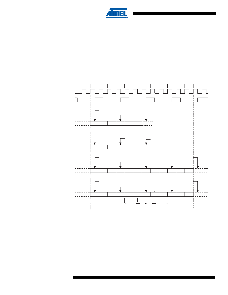
5.2
Compatibility Mode
Compatibility (12-Clock) mode is enabled by default from the factory or by setting the Compati-
bility User Fuse. In Compatibility mode instruction bytes are fetched every three system clock
cycles and the CPU operates with 6-state machine cycles and a divide-by-2 system clock for 12
oscillator periods per machine cycle. Standard instructions execute in1, 2 or 4 machine cycles.
Instruction timing in this mode is compatible with standard 8051s such as the AT89S51/52.
Compatibility mode can be used to preserve the execution profiles of legacy applications. For a
summary of differences between Fast and Compatibility modes see Table 2-3 on page 10.
Examples of Compatibility mode instructions are shown in Figure 5-2.
Figure 5-2.
Instruction Execution Sequences in Compatibility Mode
5.3
Enhanced Dual Data Pointers
The AT89LP51/52 provides two 16-bit data pointers: DPTR0 formed by the register pair DPOL
and DPOH (82H an 83H), and DPTR1 formed by the register pair DP1L and DP1H (84H and
85H). The data pointers are used by several instructions to access the program or data memo-
ries. The Data Pointer Configuration Register (AUXR1) controls operation of the dual data
pointers (Table 5-3 on page 28). The DPS bit in AUXR1 selects which data pointer is currently
referenced by instructions including the DPTR operand. Each data pointer may be accessed at
its respective SFR addresses regardless of the DPS value. The AT89LP51/52 provides two
methods for fast context switching of the data pointers:
S1
S2
S3
S4
S5
S6
S1
S2
S3
S4
S5
S6
S1
S2
S3
S4
S5
S6
S1
S2
S3
S4
S5
S6
S1
S2
S3
S4
S5
S6
S1
S2
S3
S4
S5
S6
S1
S2
S3
S4
S5
S6
S1
S2
S3
S4
S5
S6
S1
CLK
ALE
READ OPCODE
(A) 1-byte, 1-cycle instruction, e.g., INC A
A
(B) 2-byte, 1-cycle instruction, e.g., ADD A, #data
(C) 1-byte, 2-cycle instruction, e.g., INC DPTR
(D) MOVX (1-byte, 2-cycle)
READ NEXT
OPCODE
(DISCARD)
READ NEXT OPCODE AGAIN
READ OPCODE
READ 2ND
BYTE
READ NEXT OPCODE
READ OPCODE
READ NEXT
OPCODE AGAIN
READ
OPCODE
(MOVX)
NO
ALE
READ NEXT
OPCODE (DISCARD)
READ NEXT
OPCODE
AGAIN
NO
FETCH
DA
DATA
ACCESS EXTERNAL MEMOR
ACCESS EXTERNAL MEMORY
ADDR
NO
FETCH
READ NEXT
OPCODE (DISCARD)
相关PDF资料 |
PDF描述 |
|---|---|
| VE-B7K-IX-F4 | CONVERTER MOD DC/DC 40V 75W |
| ATMEGA32L-8MU | IC AVR MCU 32K 8MHZ 3V 44-QFN |
| VE-BTJ-IW-F1 | CONVERTER MOD DC/DC 36V 100W |
| MB95F168JAPMC1-GE1 | IC MCU FLASH 60K ROM 64LQFP |
| D38999/26MB5SA | CONN PLUG 5POS STRAIGHT W/SCKT |
相关代理商/技术参数 |
参数描述 |
|---|---|
| AT89LP51ED2-20AAU | 功能描述:8位微控制器 -MCU 64KB 20MHz 2.4V-5.5V RoHS:否 制造商:Silicon Labs 核心:8051 处理器系列:C8051F39x 数据总线宽度:8 bit 最大时钟频率:50 MHz 程序存储器大小:16 KB 数据 RAM 大小:1 KB 片上 ADC:Yes 工作电源电压:1.8 V to 3.6 V 工作温度范围:- 40 C to + 105 C 封装 / 箱体:QFN-20 安装风格:SMD/SMT |
| AT89LP51ED2-20AU | 功能描述:8位微控制器 -MCU 64KB 20MHz 2.4V-5.5V RoHS:否 制造商:Silicon Labs 核心:8051 处理器系列:C8051F39x 数据总线宽度:8 bit 最大时钟频率:50 MHz 程序存储器大小:16 KB 数据 RAM 大小:1 KB 片上 ADC:Yes 工作电源电压:1.8 V to 3.6 V 工作温度范围:- 40 C to + 105 C 封装 / 箱体:QFN-20 安装风格:SMD/SMT |
| AT89LP51ED2-20JU | 功能描述:8位微控制器 -MCU 64KB 20MHz 2.4V-5.5V RoHS:否 制造商:Silicon Labs 核心:8051 处理器系列:C8051F39x 数据总线宽度:8 bit 最大时钟频率:50 MHz 程序存储器大小:16 KB 数据 RAM 大小:1 KB 片上 ADC:Yes 工作电源电压:1.8 V to 3.6 V 工作温度范围:- 40 C to + 105 C 封装 / 箱体:QFN-20 安装风格:SMD/SMT |
| AT89LP51ED2-20MU | 功能描述:8位微控制器 -MCU 64KB 20MHz 2.4V-5.5V RoHS:否 制造商:Silicon Labs 核心:8051 处理器系列:C8051F39x 数据总线宽度:8 bit 最大时钟频率:50 MHz 程序存储器大小:16 KB 数据 RAM 大小:1 KB 片上 ADC:Yes 工作电源电压:1.8 V to 3.6 V 工作温度范围:- 40 C to + 105 C 封装 / 箱体:QFN-20 安装风格:SMD/SMT |
| AT89LP51ED2-20PU | 功能描述:8位微控制器 -MCU 64KB 20MHz 2.4V-5.5V RoHS:否 制造商:Silicon Labs 核心:8051 处理器系列:C8051F39x 数据总线宽度:8 bit 最大时钟频率:50 MHz 程序存储器大小:16 KB 数据 RAM 大小:1 KB 片上 ADC:Yes 工作电源电压:1.8 V to 3.6 V 工作温度范围:- 40 C to + 105 C 封装 / 箱体:QFN-20 安装风格:SMD/SMT |
发布紧急采购,3分钟左右您将得到回复。