- 您现在的位置:买卖IC网 > PDF目录11722 > AT89LP51-20PU (Atmel)MCU 8051 4K FLASH 20MHZ PDF资料下载
参数资料
| 型号: | AT89LP51-20PU |
| 厂商: | Atmel |
| 文件页数: | 45/117页 |
| 文件大小: | 0K |
| 描述: | MCU 8051 4K FLASH 20MHZ |
| 标准包装: | 10 |
| 系列: | 89LP |
| 核心处理器: | 8051 |
| 芯体尺寸: | 8-位 |
| 速度: | 20MHz |
| 连通性: | EBI/EMI,I²C,SPI,UART/USART |
| 外围设备: | 欠压检测/复位,POR,PWM,WDT |
| 输入/输出数: | 36 |
| 程序存储器容量: | 4KB(4K x 8) |
| 程序存储器类型: | 闪存 |
| RAM 容量: | 256 x 8 |
| 电压 - 电源 (Vcc/Vdd): | 2.4 V ~ 5.5 V |
| 振荡器型: | 内部 |
| 工作温度: | -40°C ~ 85°C |
| 封装/外壳: | 40-DIP(0.600",15.24mm) |
| 包装: | 管件 |
第1页第2页第3页第4页第5页第6页第7页第8页第9页第10页第11页第12页第13页第14页第15页第16页第17页第18页第19页第20页第21页第22页第23页第24页第25页第26页第27页第28页第29页第30页第31页第32页第33页第34页第35页第36页第37页第38页第39页第40页第41页第42页第43页第44页当前第45页第46页第47页第48页第49页第50页第51页第52页第53页第54页第55页第56页第57页第58页第59页第60页第61页第62页第63页第64页第65页第66页第67页第68页第69页第70页第71页第72页第73页第74页第75页第76页第77页第78页第79页第80页第81页第82页第83页第84页第85页第86页第87页第88页第89页第90页第91页第92页第93页第94页第95页第96页第97页第98页第99页第100页第101页第102页第103页第104页第105页第106页第107页第108页第109页第110页第111页第112页第113页第114页第115页第116页第117页
33
3709D–MICRO–12/11
AT89LP51/52
7.2
Brown-out Reset
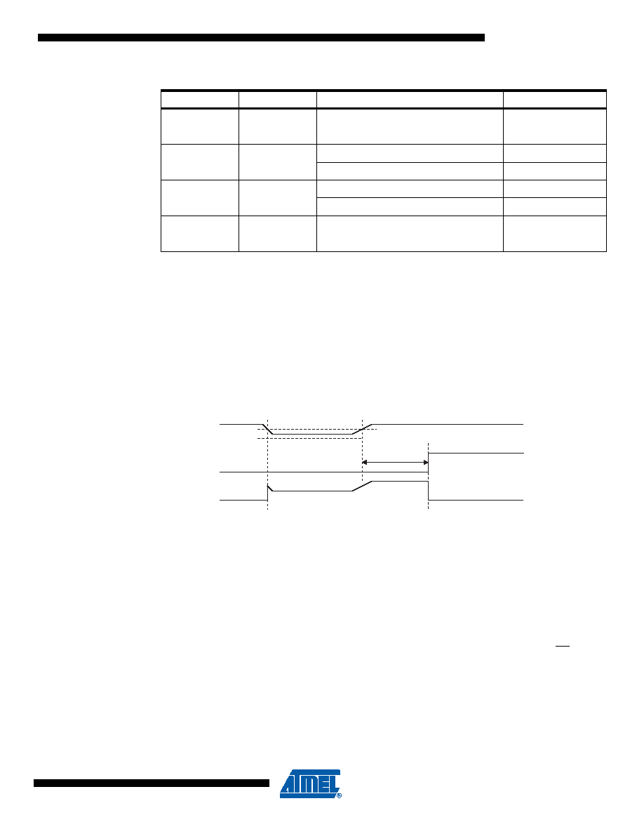
The AT89LP51/52 has an on-chip Brown-out Detection (BOD) circuit for monitoring the V
DD level
during operation by comparing it to a fixed trigger level. The trigger level V
BOD for the BOD is
nominally 2.0V. The purpose of the BOD is to ensure that if V
DD fails or dips while executing at
speed, the system will gracefully enter reset without the possibility of errors induced by incorrect
execution. A BOD sequence is shown in Figure 7-2. When V
DD decreases to a value below the
trigger level V
BOD, the internal reset is immediately activated. When VDD increases above the
trigger level plus about 200 mV of hysteresis, the start-up timer releases the internal reset after
the specified time-out period has expired (Table 7-1).
Figure 7-2.
Brown-out Detector Reset
The AT89LP51/52 allows for a wide V
DD operating range. The on-chip BOD may not be suffi-
cient to prevent incorrect execution if V
BOD is lower than the minimum required VDD range, such
as when a 5.0V supply is coupled with high frequency operation. In such cases an external
Brown-out Reset circuit connected to the RST pin may be required.
7.3
External Reset
The RST pin of the AT89LP51/52 can function as either an active-low reset input or as an active-
high reset input. The polarity of the RST pin is selectable using the POL pin (formerly EA). When
POL is high the RST pin is active high with an on-chip pull-down resistor tied to GND. When
POL is low the RST pin is active low with an on-chip pull-up resistor tied to V
DD. The RST pin
structure is shown in Figure 7-3. In Compatibility mode the reset pin is sampled every six clock
cycles and must be held active for at least twelve clock cycles to trigger the internal reset. In
Fast mode the reset pin is sampled every clock cycle and must be held active for at least two
clock cycles to trigger the internal reset.
Table 7-1.
Start-up Timer Settings
SUT Fuse 1
SUT Fuse 0
Clock Source
t
SUT (± 5%) s
00
Internal RC/External Clock
16
Crystal Oscillator
1024
01
Internal RC/External Clock
512
Crystal Oscillator
2048
10
Internal RC/External Clock
1024
Crystal Oscillator
4096
11
Internal RC/External Clock
4096
Crystal Oscillator
16384
VDD
Time-out
VPOR
Internal
Reset
tSUT
VBOD
相关PDF资料 |
PDF描述 |
|---|---|
| VE-B7K-IX-F4 | CONVERTER MOD DC/DC 40V 75W |
| ATMEGA32L-8MU | IC AVR MCU 32K 8MHZ 3V 44-QFN |
| VE-BTJ-IW-F1 | CONVERTER MOD DC/DC 36V 100W |
| MB95F168JAPMC1-GE1 | IC MCU FLASH 60K ROM 64LQFP |
| D38999/26MB5SA | CONN PLUG 5POS STRAIGHT W/SCKT |
相关代理商/技术参数 |
参数描述 |
|---|---|
| AT89LP51ED2-20AAU | 功能描述:8位微控制器 -MCU 64KB 20MHz 2.4V-5.5V RoHS:否 制造商:Silicon Labs 核心:8051 处理器系列:C8051F39x 数据总线宽度:8 bit 最大时钟频率:50 MHz 程序存储器大小:16 KB 数据 RAM 大小:1 KB 片上 ADC:Yes 工作电源电压:1.8 V to 3.6 V 工作温度范围:- 40 C to + 105 C 封装 / 箱体:QFN-20 安装风格:SMD/SMT |
| AT89LP51ED2-20AU | 功能描述:8位微控制器 -MCU 64KB 20MHz 2.4V-5.5V RoHS:否 制造商:Silicon Labs 核心:8051 处理器系列:C8051F39x 数据总线宽度:8 bit 最大时钟频率:50 MHz 程序存储器大小:16 KB 数据 RAM 大小:1 KB 片上 ADC:Yes 工作电源电压:1.8 V to 3.6 V 工作温度范围:- 40 C to + 105 C 封装 / 箱体:QFN-20 安装风格:SMD/SMT |
| AT89LP51ED2-20JU | 功能描述:8位微控制器 -MCU 64KB 20MHz 2.4V-5.5V RoHS:否 制造商:Silicon Labs 核心:8051 处理器系列:C8051F39x 数据总线宽度:8 bit 最大时钟频率:50 MHz 程序存储器大小:16 KB 数据 RAM 大小:1 KB 片上 ADC:Yes 工作电源电压:1.8 V to 3.6 V 工作温度范围:- 40 C to + 105 C 封装 / 箱体:QFN-20 安装风格:SMD/SMT |
| AT89LP51ED2-20MU | 功能描述:8位微控制器 -MCU 64KB 20MHz 2.4V-5.5V RoHS:否 制造商:Silicon Labs 核心:8051 处理器系列:C8051F39x 数据总线宽度:8 bit 最大时钟频率:50 MHz 程序存储器大小:16 KB 数据 RAM 大小:1 KB 片上 ADC:Yes 工作电源电压:1.8 V to 3.6 V 工作温度范围:- 40 C to + 105 C 封装 / 箱体:QFN-20 安装风格:SMD/SMT |
| AT89LP51ED2-20PU | 功能描述:8位微控制器 -MCU 64KB 20MHz 2.4V-5.5V RoHS:否 制造商:Silicon Labs 核心:8051 处理器系列:C8051F39x 数据总线宽度:8 bit 最大时钟频率:50 MHz 程序存储器大小:16 KB 数据 RAM 大小:1 KB 片上 ADC:Yes 工作电源电压:1.8 V to 3.6 V 工作温度范围:- 40 C to + 105 C 封装 / 箱体:QFN-20 安装风格:SMD/SMT |
发布紧急采购,3分钟左右您将得到回复。