- 您现在的位置:买卖IC网 > PDF目录11722 > AT89LP51-20PU (Atmel)MCU 8051 4K FLASH 20MHZ PDF资料下载
参数资料
| 型号: | AT89LP51-20PU |
| 厂商: | Atmel |
| 文件页数: | 78/117页 |
| 文件大小: | 0K |
| 描述: | MCU 8051 4K FLASH 20MHZ |
| 标准包装: | 10 |
| 系列: | 89LP |
| 核心处理器: | 8051 |
| 芯体尺寸: | 8-位 |
| 速度: | 20MHz |
| 连通性: | EBI/EMI,I²C,SPI,UART/USART |
| 外围设备: | 欠压检测/复位,POR,PWM,WDT |
| 输入/输出数: | 36 |
| 程序存储器容量: | 4KB(4K x 8) |
| 程序存储器类型: | 闪存 |
| RAM 容量: | 256 x 8 |
| 电压 - 电源 (Vcc/Vdd): | 2.4 V ~ 5.5 V |
| 振荡器型: | 内部 |
| 工作温度: | -40°C ~ 85°C |
| 封装/外壳: | 40-DIP(0.600",15.24mm) |
| 包装: | 管件 |
第1页第2页第3页第4页第5页第6页第7页第8页第9页第10页第11页第12页第13页第14页第15页第16页第17页第18页第19页第20页第21页第22页第23页第24页第25页第26页第27页第28页第29页第30页第31页第32页第33页第34页第35页第36页第37页第38页第39页第40页第41页第42页第43页第44页第45页第46页第47页第48页第49页第50页第51页第52页第53页第54页第55页第56页第57页第58页第59页第60页第61页第62页第63页第64页第65页第66页第67页第68页第69页第70页第71页第72页第73页第74页第75页第76页第77页当前第78页第79页第80页第81页第82页第83页第84页第85页第86页第87页第88页第89页第90页第91页第92页第93页第94页第95页第96页第97页第98页第99页第100页第101页第102页第103页第104页第105页第106页第107页第108页第109页第110页第111页第112页第113页第114页第115页第116页第117页
63
3709D–MICRO–12/11
AT89LP51/52
The Broadcast Address for each slave is created by taking the logic OR of SADDR and SADEN.
Zeros in this result are trended as don’t cares. In most cases, interpreting the don’t cares as
ones, the broadcast address will be FF hexadecimal.
Upon reset SADDR (SFR address 0A9H) and SADEN (SFR address 0B9H) are loaded with
“0”s. This produces a given address of all “don’t cares” as well as a Broadcast address of all
“don’t cares”. This effectively disables the Automatic Addressing mode and allows the microcon-
troller to use standard 80C51-type UART drivers which do not make use of this feature.
14.5
More About Mode 0
In Mode 0, the UART is configured as either a two wire half-duplex or three wire full-duplex syn-
chronous serial interface. In two-wire mode serial data enters and exits through RXD and TXD
outputs the shift clock. In three-wire mode serial data enters through MISO, exits through MOSI
and SCK outputs the shift clock. Eight data bits are transmitted/received, with the LSB first. Fig-
ure 14-3 and Figure 14-5 on page 67 show simplified functional diagrams of the serial port in
Mode 0 and associated timing. The baud rate is programmable to 1/2 or 1/4 the system fre-
quency by setting/clearing the SMOD1 bit in Fast mode, or 1/3 or 1/6 the system frequency in
Compatibility mode. However, changing SMOD1 has an effect on the relationship between the
clock and data as described below. The baud rate can also be generated by Timer 1 by setting
TB8. Table 14-4 lists the baud rate options for Mode 0.
14.5.1
Two-Wire (Half-Duplex) Mode
Transmission is initiated by any instruction that uses SBUF as a destination register. The “write
to SBUF” signal also loads a “1” into the 9th position of the transmit shift register and tells the TX
Control Block to begin a transmission. The internal timing is such that one full bit slot may elapse
between “write to SBUF” and activation of SEND.
SEND transfers the output of the shift register to the alternate output function line of P3.0, and
also transfers Shift Clock to the alternate output function line of P3.1. As data bits shift out to the
right, “0”s come in from the left. When the MSB of the data byte is at the output position of the
shift register, the “1” that was initially loaded into the 9th position is just to the left of the MSB,
and all positions to the left of that contain “0”s. This condition flags the TX Control block to do
one last shift, then deactivate SEND and set TI.
Reception is initiated by the condition REN = 1 and RI = 0. At the next clock cycle, the RX Con-
trol unit writes the bits 11111110B to the receive shift register and activates RECEIVE in the
next clock phase. RECEIVE enables Shift Clock to the alternate output function line of P3.1. As
data bits come in from the right, “1”s shift out to the left. When the “0” that was initially loaded
into the right-most position arrives at the left-most position in the shift register, it flags the RX
Control block to do one last shift and load SBUF. Then RECEIVE is cleared and RI is set.
The relationship between the shift clock and data is determined by the combination of the SM2
and SMOD1 bits as listed in Table 14-5 and shown in Figure . The SM2 bit determines the idle
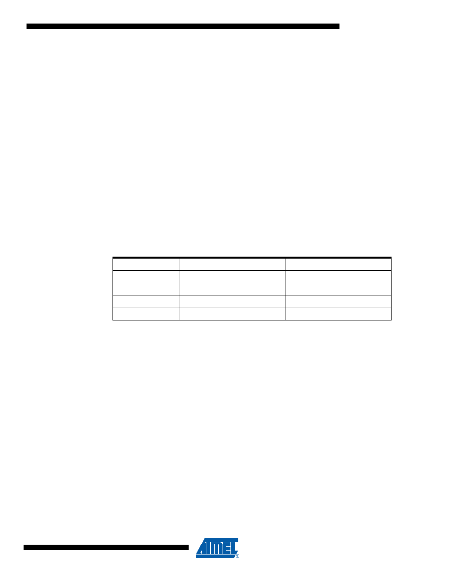
Table 14-4.
Mode 0 Baud Rates
TB8
SMOD1
Baud Rate (Fast)
Baud Rate (Compatibility)
00
fSYS/4
fSYS/6
01
fSYS/2
fSYS/3
1
0
(Timer 1 Overflow) / 4
1
(Timer 1 Overflow) / 2
相关PDF资料 |
PDF描述 |
|---|---|
| VE-B7K-IX-F4 | CONVERTER MOD DC/DC 40V 75W |
| ATMEGA32L-8MU | IC AVR MCU 32K 8MHZ 3V 44-QFN |
| VE-BTJ-IW-F1 | CONVERTER MOD DC/DC 36V 100W |
| MB95F168JAPMC1-GE1 | IC MCU FLASH 60K ROM 64LQFP |
| D38999/26MB5SA | CONN PLUG 5POS STRAIGHT W/SCKT |
相关代理商/技术参数 |
参数描述 |
|---|---|
| AT89LP51ED2-20AAU | 功能描述:8位微控制器 -MCU 64KB 20MHz 2.4V-5.5V RoHS:否 制造商:Silicon Labs 核心:8051 处理器系列:C8051F39x 数据总线宽度:8 bit 最大时钟频率:50 MHz 程序存储器大小:16 KB 数据 RAM 大小:1 KB 片上 ADC:Yes 工作电源电压:1.8 V to 3.6 V 工作温度范围:- 40 C to + 105 C 封装 / 箱体:QFN-20 安装风格:SMD/SMT |
| AT89LP51ED2-20AU | 功能描述:8位微控制器 -MCU 64KB 20MHz 2.4V-5.5V RoHS:否 制造商:Silicon Labs 核心:8051 处理器系列:C8051F39x 数据总线宽度:8 bit 最大时钟频率:50 MHz 程序存储器大小:16 KB 数据 RAM 大小:1 KB 片上 ADC:Yes 工作电源电压:1.8 V to 3.6 V 工作温度范围:- 40 C to + 105 C 封装 / 箱体:QFN-20 安装风格:SMD/SMT |
| AT89LP51ED2-20JU | 功能描述:8位微控制器 -MCU 64KB 20MHz 2.4V-5.5V RoHS:否 制造商:Silicon Labs 核心:8051 处理器系列:C8051F39x 数据总线宽度:8 bit 最大时钟频率:50 MHz 程序存储器大小:16 KB 数据 RAM 大小:1 KB 片上 ADC:Yes 工作电源电压:1.8 V to 3.6 V 工作温度范围:- 40 C to + 105 C 封装 / 箱体:QFN-20 安装风格:SMD/SMT |
| AT89LP51ED2-20MU | 功能描述:8位微控制器 -MCU 64KB 20MHz 2.4V-5.5V RoHS:否 制造商:Silicon Labs 核心:8051 处理器系列:C8051F39x 数据总线宽度:8 bit 最大时钟频率:50 MHz 程序存储器大小:16 KB 数据 RAM 大小:1 KB 片上 ADC:Yes 工作电源电压:1.8 V to 3.6 V 工作温度范围:- 40 C to + 105 C 封装 / 箱体:QFN-20 安装风格:SMD/SMT |
| AT89LP51ED2-20PU | 功能描述:8位微控制器 -MCU 64KB 20MHz 2.4V-5.5V RoHS:否 制造商:Silicon Labs 核心:8051 处理器系列:C8051F39x 数据总线宽度:8 bit 最大时钟频率:50 MHz 程序存储器大小:16 KB 数据 RAM 大小:1 KB 片上 ADC:Yes 工作电源电压:1.8 V to 3.6 V 工作温度范围:- 40 C to + 105 C 封装 / 箱体:QFN-20 安装风格:SMD/SMT |
发布紧急采购,3分钟左右您将得到回复。