- 您现在的位置:买卖IC网 > PDF目录11722 > AT89LP51-20PU (Atmel)MCU 8051 4K FLASH 20MHZ PDF资料下载
参数资料
| 型号: | AT89LP51-20PU |
| 厂商: | Atmel |
| 文件页数: | 81/117页 |
| 文件大小: | 0K |
| 描述: | MCU 8051 4K FLASH 20MHZ |
| 标准包装: | 10 |
| 系列: | 89LP |
| 核心处理器: | 8051 |
| 芯体尺寸: | 8-位 |
| 速度: | 20MHz |
| 连通性: | EBI/EMI,I²C,SPI,UART/USART |
| 外围设备: | 欠压检测/复位,POR,PWM,WDT |
| 输入/输出数: | 36 |
| 程序存储器容量: | 4KB(4K x 8) |
| 程序存储器类型: | 闪存 |
| RAM 容量: | 256 x 8 |
| 电压 - 电源 (Vcc/Vdd): | 2.4 V ~ 5.5 V |
| 振荡器型: | 内部 |
| 工作温度: | -40°C ~ 85°C |
| 封装/外壳: | 40-DIP(0.600",15.24mm) |
| 包装: | 管件 |
第1页第2页第3页第4页第5页第6页第7页第8页第9页第10页第11页第12页第13页第14页第15页第16页第17页第18页第19页第20页第21页第22页第23页第24页第25页第26页第27页第28页第29页第30页第31页第32页第33页第34页第35页第36页第37页第38页第39页第40页第41页第42页第43页第44页第45页第46页第47页第48页第49页第50页第51页第52页第53页第54页第55页第56页第57页第58页第59页第60页第61页第62页第63页第64页第65页第66页第67页第68页第69页第70页第71页第72页第73页第74页第75页第76页第77页第78页第79页第80页当前第81页第82页第83页第84页第85页第86页第87页第88页第89页第90页第91页第92页第93页第94页第95页第96页第97页第98页第99页第100页第101页第102页第103页第104页第105页第106页第107页第108页第109页第110页第111页第112页第113页第114页第115页第116页第117页
66
3709D–MICRO–12/11
AT89LP51/52
Mode 0 transfers data LSB first whereas SPI or TWI are generally MSB first. Emulation of these
interfaces may require bit reversal of the transferred data bytes. The following code example
reverses the bits in the accumulator:
EX:
MOV
R7, #8
REVRS: RLC
A
; C << msb (ACC)
XCH
A, R6
RRC
A
; msb (ACC) >> B
XCH
A, R6
DJNZ R7, REVRS
14.5.2
Three-Wire (Full-Duplex) Mode
Three-Wire Mode is similar to Two-Wire except that the shift data input and data output are sep-
arated for full-duplex operation. Three-Wire Mode is enabled by setting the SPEN bit in TCONB.
Transmission is initiated by any instruction that uses SBUF as a destination register. The “write
to SBUF” signal also loads a “1” into the 9th position of the transmit shift register and tells the TX
Control Block to begin a transmission. The internal timing is such that one full bit slot may elapse
between “write to SBUF” and activation of SEND.
SEND transfers the output of the shift register to the alternate output function line of P1.5, and
also transfers Shift Clock to the alternate output function line of P1.7. As data bits shift out to the
right, “0”s come in from the left. When the MSB of the data byte is at the output position of the
shift register, the “1” that was initially loaded into the 9th position is just to the left of the MSB,
and all positions to the left of that contain “0”s. This condition flags the TX Control block to do
one last shift, then deactivate SEND and set TI.
Reception occurs simultaneously with transmission if REN = 1. Data is input from P1.6. When
REN = 1 any write to SBUF causes the RX Control unit to write the bits 11111110B to the
receive shift register and activates RECEIVE in the next clock phase. As data bits come in from
the right, “1”s shift out to the left. When the “0” that was initially loaded into the right-most posi-
tion arrives at the left-most position in the shift register, it flags the RX Control block to do one
last shift and load SBUF. Then RECEIVE is cleared and RI is set. When REN = 0, the receiver is
not enabled. When a transmission occurs, SBUF will not be updated and RI will not be set even
though serial data is received on P1.6.
The relationship between the shift clock and data is identical to Two-Wire mode as listed in
Table 14-5 and shown in Figure . Three-Wire mode uses different I/Os from Two-Wire mode and
can be connected to SPI slave devices as shownin Figure 14-4. It is possible to time share the
UART hardware between SPI devices connected on P1 and UART devices on P3 with the
caveat that any asynchronous receptions on the RXD pin will be ignored while the UART is in
Mode 0.
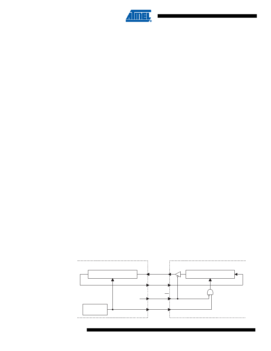
Figure 14-4. SPI Connections for UART Mode 0
8-Bit Shift Register
Master
Slave
MSB
LSB
MSB
LSB
8-Bit Shift Register
MISO
MOSI
SS
GPIO
SCK
Clock
Generator
AT89LP52
相关PDF资料 |
PDF描述 |
|---|---|
| VE-B7K-IX-F4 | CONVERTER MOD DC/DC 40V 75W |
| ATMEGA32L-8MU | IC AVR MCU 32K 8MHZ 3V 44-QFN |
| VE-BTJ-IW-F1 | CONVERTER MOD DC/DC 36V 100W |
| MB95F168JAPMC1-GE1 | IC MCU FLASH 60K ROM 64LQFP |
| D38999/26MB5SA | CONN PLUG 5POS STRAIGHT W/SCKT |
相关代理商/技术参数 |
参数描述 |
|---|---|
| AT89LP51ED2-20AAU | 功能描述:8位微控制器 -MCU 64KB 20MHz 2.4V-5.5V RoHS:否 制造商:Silicon Labs 核心:8051 处理器系列:C8051F39x 数据总线宽度:8 bit 最大时钟频率:50 MHz 程序存储器大小:16 KB 数据 RAM 大小:1 KB 片上 ADC:Yes 工作电源电压:1.8 V to 3.6 V 工作温度范围:- 40 C to + 105 C 封装 / 箱体:QFN-20 安装风格:SMD/SMT |
| AT89LP51ED2-20AU | 功能描述:8位微控制器 -MCU 64KB 20MHz 2.4V-5.5V RoHS:否 制造商:Silicon Labs 核心:8051 处理器系列:C8051F39x 数据总线宽度:8 bit 最大时钟频率:50 MHz 程序存储器大小:16 KB 数据 RAM 大小:1 KB 片上 ADC:Yes 工作电源电压:1.8 V to 3.6 V 工作温度范围:- 40 C to + 105 C 封装 / 箱体:QFN-20 安装风格:SMD/SMT |
| AT89LP51ED2-20JU | 功能描述:8位微控制器 -MCU 64KB 20MHz 2.4V-5.5V RoHS:否 制造商:Silicon Labs 核心:8051 处理器系列:C8051F39x 数据总线宽度:8 bit 最大时钟频率:50 MHz 程序存储器大小:16 KB 数据 RAM 大小:1 KB 片上 ADC:Yes 工作电源电压:1.8 V to 3.6 V 工作温度范围:- 40 C to + 105 C 封装 / 箱体:QFN-20 安装风格:SMD/SMT |
| AT89LP51ED2-20MU | 功能描述:8位微控制器 -MCU 64KB 20MHz 2.4V-5.5V RoHS:否 制造商:Silicon Labs 核心:8051 处理器系列:C8051F39x 数据总线宽度:8 bit 最大时钟频率:50 MHz 程序存储器大小:16 KB 数据 RAM 大小:1 KB 片上 ADC:Yes 工作电源电压:1.8 V to 3.6 V 工作温度范围:- 40 C to + 105 C 封装 / 箱体:QFN-20 安装风格:SMD/SMT |
| AT89LP51ED2-20PU | 功能描述:8位微控制器 -MCU 64KB 20MHz 2.4V-5.5V RoHS:否 制造商:Silicon Labs 核心:8051 处理器系列:C8051F39x 数据总线宽度:8 bit 最大时钟频率:50 MHz 程序存储器大小:16 KB 数据 RAM 大小:1 KB 片上 ADC:Yes 工作电源电压:1.8 V to 3.6 V 工作温度范围:- 40 C to + 105 C 封装 / 箱体:QFN-20 安装风格:SMD/SMT |
发布紧急采购,3分钟左右您将得到回复。