- 您现在的位置:买卖IC网 > PDF目录256005 > BX80532KC3000D (INTEL CORP) 3000 MHz, MICROPROCESSOR PDF资料下载
参数资料
| 型号: | BX80532KC3000D |
| 厂商: | INTEL CORP |
| 元件分类: | 微控制器/微处理器 |
| 英文描述: | 3000 MHz, MICROPROCESSOR |
| 文件页数: | 112/129页 |
| 文件大小: | 1640K |
| 代理商: | BX80532KC3000D |
第1页第2页第3页第4页第5页第6页第7页第8页第9页第10页第11页第12页第13页第14页第15页第16页第17页第18页第19页第20页第21页第22页第23页第24页第25页第26页第27页第28页第29页第30页第31页第32页第33页第34页第35页第36页第37页第38页第39页第40页第41页第42页第43页第44页第45页第46页第47页第48页第49页第50页第51页第52页第53页第54页第55页第56页第57页第58页第59页第60页第61页第62页第63页第64页第65页第66页第67页第68页第69页第70页第71页第72页第73页第74页第75页第76页第77页第78页第79页第80页第81页第82页第83页第84页第85页第86页第87页第88页第89页第90页第91页第92页第93页第94页第95页第96页第97页第98页第99页第100页第101页第102页第103页第104页第105页第106页第107页第108页第109页第110页第111页当前第112页第113页第114页第115页第116页第117页第118页第119页第120页第121页第122页第123页第124页第125页第126页第127页第128页第129页
Intel Xeon Processor with 512 KB L2 Cache
Datasheet
83
1. These are “Reserved” pins on the Intel Xeon processor. In
systems utilizing the Intel Xeon processor, the system
designer must terminate these signals to the processor VCC.
2. Baseboards treating AA3 and AB3 as Reserved will operate
correctly with a bus clock of 100 MHz.
AC20
D25#
Source Sync
Input/Output
AC21
D26#
Source Sync
Input/Output
AC22
VCC
Power/Other
AC23
D23#
Source Sync
Input/Output
AC24
D20#
Source Sync
Input/Output
AC25
VSS
Power/Other
AC26
D17#
Source Sync
Input/Output
AC27
DBI0#
Source Sync
Input/Output
AC28
SM_CLK
SMBus
Input
AC29
SM_DAT
SMBus
Output
AC30
VSS
Power/Other
AC31
VCC
Power/Other
AD1
Reserved
AD2
VCC
Power/Other
AD3
VSS
Power/Other
AD4
VCCIOPLL
Power/Other
Input
AD5
TESTHI5
Power/Other
Input
AD6
VCC
Power/Other
AD7
D57#
Source Sync
Input/Output
AD8
D46#
Source Sync
Input/Output
AD9
VSS
Power/Other
AD10
D45#
Source Sync
Input/Output
AD11
D40#
Source Sync
Input/Output
AD12
VCC
Power/Other
AD13
D38#
Source Sync
Input/Output
AD14
D39#
Source Sync
Input/Output
AD15
VSS
Power/Other
AD16
COMP0
Power/Other
Input
AD17
VSS
Power/Other
AD18
D36#
Source Sync
Input/Output
AD19
D30#
Source Sync
Input/Output
AD20
VCC
Power/Other
AD21
D29#
Source Sync
Input/Output
AD22
DBI1#
Source Sync
Input/Output
AD23
VSS
Power/Other
AD24
D21#
Source Sync
Input/Output
AD25
D18#
Source Sync
Input/Output
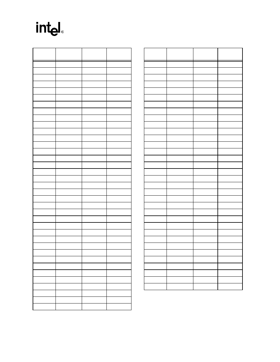
Table 39. Pin Listing by Pin Number
Pin No.
Pin Name
Signal
Buffer Type
Direction
AD26
VCC
Power/Other
AD27
D4#
Source Sync
Input/Output
AD28
SM_ALERT#
SMBus
Output
AD29
SM_WP
SMBus
Input
AD30
VCC
Power/Other
AD31
VSS
Power/Other
AE2
VSS
Power/Other
AE3
VCC
Power/Other
AE4
Reserved
AE5
TESTHI6
Power/Other
Input
AE6
SLP#
Async GTL+
Input
AE7
D58#
Source Sync
Input/Output
AE8
VCC
Power/Other
AE9
D44#
Source Sync
Input/Output
AE10
D42#
Source Sync
Input/Output
AE11
VSS
Power/Other
AE12
DBI2#
Source Sync
Input/Output
AE13
D35#
Source Sync
Input/Output
AE14
VCC
Power/Other
AE15
Reserved
AE16
Reserved
AE17
DP3#
Common Clk
Input/Output
AE18
VCC
Power/Other
AE19
DP1#
Common Clk
Input/Output
AE20
D28#
Source Sync
Input/Output
AE21
VSS
Power/Other
AE22
D27#
Source Sync
Input/Output
AE23
D22#
Source Sync
Input/Output
AE24
VCC
Power/Other
AE25
D19#
Source Sync
Input/Output
AE26
D16#
Source Sync
Input/Output
AE27
VSS
Power/Other
AE28
SM_VCC
Power/Other
AE29
SM_VCC
Power/Other
Table 39. Pin Listing by Pin Number
Pin No.
Pin Name
Signal
Buffer Type
Direction
相关PDF资料 |
PDF描述 |
|---|---|
| BU-65843F3-110 | 2 CHANNEL(S), 1M bps, MIL-STD-1553 CONTROLLER, CQFP80 |
| BP83C51FA-1 | 8-BIT, MROM, 16 MHz, MICROCONTROLLER, PDIP40 |
| BU-61559D1-240S | 2 CHANNEL(S), 1M bps, MIL-STD-1553 CONTROLLER, CQIP78 |
| BU-61559D1-240 | 2 CHANNEL(S), 1M bps, MIL-STD-1553 CONTROLLER, CQIP78 |
| BU-61559D1-290K | 2 CHANNEL(S), 1M bps, MIL-STD-1553 CONTROLLER, CQIP78 |
相关代理商/技术参数 |
参数描述 |
|---|---|
| BX80532KC3000H | 制造商:Intel 功能描述:MPU XEON NETBURST 64-BIT 0.13UM 3GHZ - Boxed Product (Development Kits) |
| BX80532KE2000D | 制造商:Intel 功能描述:MPU XEON PROCESSOR NETBURST 64-BIT 0.13UM 2GHZ - Boxed Product (Development Kits) |
| BX80532KE2000DU | 制造商:Intel 功能描述:XEON 2.0GHZ 533FSB 1U - Boxed Product (Development Kits) |
| BX80532KE2400DSL73L | 制造商:Intel 功能描述: |
| BX80532KE2400E | 制造商:Intel 功能描述:MPU XEON PROCESSOR NETBURST 64-BIT 0.13UM 2.4GHZ - Boxed Product (Development Kits) |
发布紧急采购,3分钟左右您将得到回复。