- 您现在的位置:买卖IC网 > PDF目录212189 > DDC118IRTCT (TEXAS INSTRUMENTS INC) 8-CH 20-BIT DELTA-SIGMA ADC, SERIAL ACCESS, PQCC48 PDF资料下载
参数资料
| 型号: | DDC118IRTCT |
| 厂商: | TEXAS INSTRUMENTS INC |
| 元件分类: | ADC |
| 英文描述: | 8-CH 20-BIT DELTA-SIGMA ADC, SERIAL ACCESS, PQCC48 |
| 封装: | GREEN, PLASTIC, QFN-48 |
| 文件页数: | 14/35页 |
| 文件大小: | 653K |
| 代理商: | DDC118IRTCT |
第1页第2页第3页第4页第5页第6页第7页第8页第9页第10页第11页第12页第13页当前第14页第15页第16页第17页第18页第19页第20页第21页第22页第23页第24页第25页第26页第27页第28页第29页第30页第31页第32页第33页第34页第35页
DDC118
SBAS325B JUNE 2004 REVISED APRIL 2009
www.ti.com
21
DATA FORMAT (FORMAT)
The serial output data is provided in an offset binary code
as shown in Table 9. The digital input pin FORMAT selects
how many bits are used in the output word. When
FORMAT is high (1), 20 bits are used. When FORMAT is
low (0), the lower 4 bits are truncated so that only 16 bits
are used. Note that the LSB size is 16 times bigger when
FORMAT = 0. An offset is included in the output to allow
slightly negative inputs, from board leakages for example,
from clipping the reading. This offset is approximately
0.4% of the positive full-scale.
Table 9. Ideal Output Code(1) vs Input Signal
INPUT
SIGNAL
IDEAL OUTPUT CODE
FORMAT = HIGH
(1)
IDEAL OUTPUT CODE
FORMAT = LOW
(0)
≥ 100% FS
1111 1111 1111 1111 1111
1111 1111 1111 1111
0.001531% FS
0000 0001 0000 0001 0000
0000 0001 0000 0001
0.001436% FS
0000 0001 0000 0000 1111
0000 0001 0000 0000
0.000191% FS
0000 0001 0000 0000 0010
0000 0001 0000 0000
0.000096% FS
0000 0001 0000 0000 0001
0000 0001 0000 0000
0% FS
0000 0001 0000 0000 0000
0000 0001 0000 0000
0.3955% FS
0000 0000 0000 0000 0000
0000 0000 0000 0000
(1) Excludes the effects of noise, INL, offset, and gain errors.
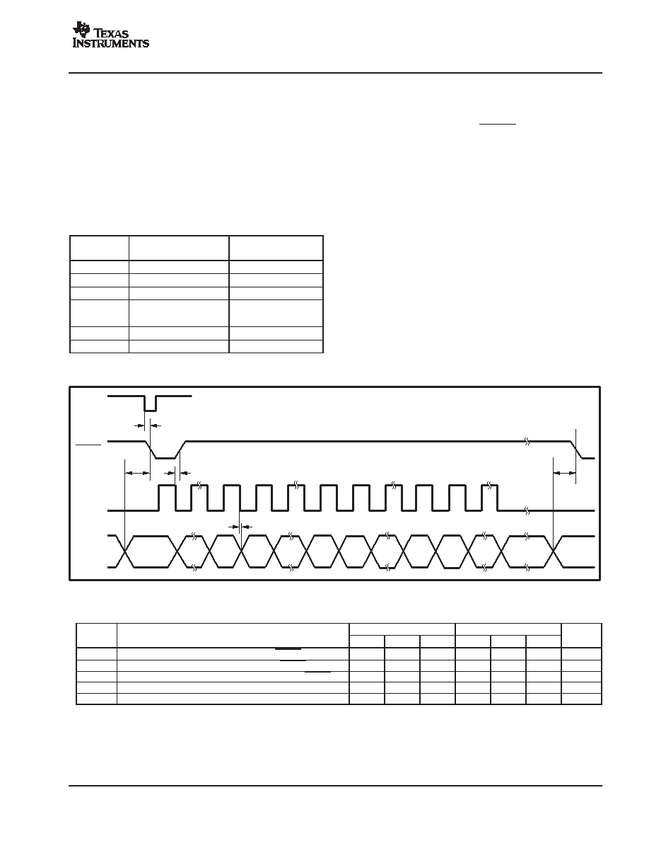
DATA RETRIEVAL
In both the continuous and non-continuous modes of
operation, the data from the last conversion is available for
retrieval on the falling edge of DVALID (see Figure 20 and
Table 10). Data is shifted out on the falling edge of the data
clock, DCLK. Make sure not to retrieve data while CONV
changes as this can introduce noise. Stop activity on
DCLK at least 10
s before or after a CONV transition.
Setting the FORMAT pin = 0 (16-bit output word) reduces
the time needed to retrieve data by 20%, since there are
fewer bits to shift out. This time reduction can be useful in
multichannel systems requiring only 16 bits of resolution.
CLK
DVALID
DCLK
DOUT
t
18
t
19
t
21
t
20
Input 8
MSB
Input 1
LSB
Input 8
LSB
Input 7
MSB
Input 5
LSB
Input 4
MSB
Input 2
LSB
Input 1
MSB
Input 8
MSB
t
20
Figure 20. Digital Interface Timing Diagram for Data Retrieval From a Single DDC118
Table 10. Timing for the DDC118 Data Retrieval
SYMBOL
DESCRIPTION
CLK = 4MHz, CLK_4X = 0
CLK = 4.8MHz, CLK_4X = 0
UNITS
SYMBOL
DESCRIPTION
MIN
TYP
MAX
MIN
TYP
MAX
UNITS
t18
Propagation Delay from Falling Edge of CLK to DVALID LOW
5
ns
t19
Propagation Delay from Falling Edge of DCLK to DVALID HIGH
5
ns
t20
Hold Time that DOUT is Valid Before the Falling Edge of DVALID
1.75
1.458
s
t21
Hold Time that DOUT is Valid After Falling Edge of DCLK
5
ns
t21A(1)
Propagation Delay from Falling Edge of DCLK to Valid DOUT
10
ns
(1) With a maximum load of one DDC118 (4pF typical) with an additional load of (5pF).
相关PDF资料 |
PDF描述 |
|---|---|
| DPB25F0/25F | 50 CONTACT(S), FEMALE-FEMALE, D SUBMINIATURE CONNECTOR, SOLDER |
| DPB25M/25M0 | 50 CONTACT(S), MALE-MALE, D SUBMINIATURE CONNECTOR, SOLDER |
| DPB25M/25M | 50 CONTACT(S), MALE-MALE, D SUBMINIATURE CONNECTOR, SOLDER |
| DPB25M0/25M0 | 50 CONTACT(S), MALE-MALE, D SUBMINIATURE CONNECTOR, SOLDER |
| DPB25M0/25M | 50 CONTACT(S), MALE-MALE, D SUBMINIATURE CONNECTOR, SOLDER |
相关代理商/技术参数 |
参数描述 |
|---|---|
| DDC118IRTCT | 制造商:Texas Instruments 功能描述:IC ADC 20BIT OCTAL 48-VQFN |
| DDC118IRTCT | 制造商:Texas Instruments 功能描述:A/D CONVERTER (A-D) IC ((NW)) |
| DDC118IRTCTG4 | 功能描述:模数转换器 - ADC Octal Current-Input 20-Bit RoHS:否 制造商:Texas Instruments 通道数量:2 结构:Sigma-Delta 转换速率:125 SPs to 8 KSPs 分辨率:24 bit 输入类型:Differential 信噪比:107 dB 接口类型:SPI 工作电源电压:1.7 V to 3.6 V, 2.7 V to 5.25 V 最大工作温度:+ 85 C 安装风格:SMD/SMT 封装 / 箱体:VQFN-32 |
| DDC11XEVM-PDK | 功能描述:数据转换 IC 开发工具 DDC11xEVM-PDK Eval Mod RoHS:否 制造商:Texas Instruments 产品:Demonstration Kits 类型:ADC 工具用于评估:ADS130E08 接口类型:SPI 工作电源电压:- 6 V to + 6 V |
| DDC122LH | 制造商:DIODES 制造商全称:Diodes Incorporated 功能描述:NPN PRE-BIASED SMALL SIGNAL SOT-563 DUAL SURFACE MOUNT TRANSISTOR |
发布紧急采购,3分钟左右您将得到回复。