- 您现在的位置:买卖IC网 > PDF目录212189 > DDC118IRTCT (TEXAS INSTRUMENTS INC) 8-CH 20-BIT DELTA-SIGMA ADC, SERIAL ACCESS, PQCC48 PDF资料下载
参数资料
| 型号: | DDC118IRTCT |
| 厂商: | TEXAS INSTRUMENTS INC |
| 元件分类: | ADC |
| 英文描述: | 8-CH 20-BIT DELTA-SIGMA ADC, SERIAL ACCESS, PQCC48 |
| 封装: | GREEN, PLASTIC, QFN-48 |
| 文件页数: | 23/35页 |
| 文件大小: | 653K |
| 代理商: | DDC118IRTCT |
第1页第2页第3页第4页第5页第6页第7页第8页第9页第10页第11页第12页第13页第14页第15页第16页第17页第18页第19页第20页第21页第22页当前第23页第24页第25页第26页第27页第28页第29页第30页第31页第32页第33页第34页第35页
DDC118
SBAS325B JUNE 2004 REVISED APRIL 2009
www.ti.com
3
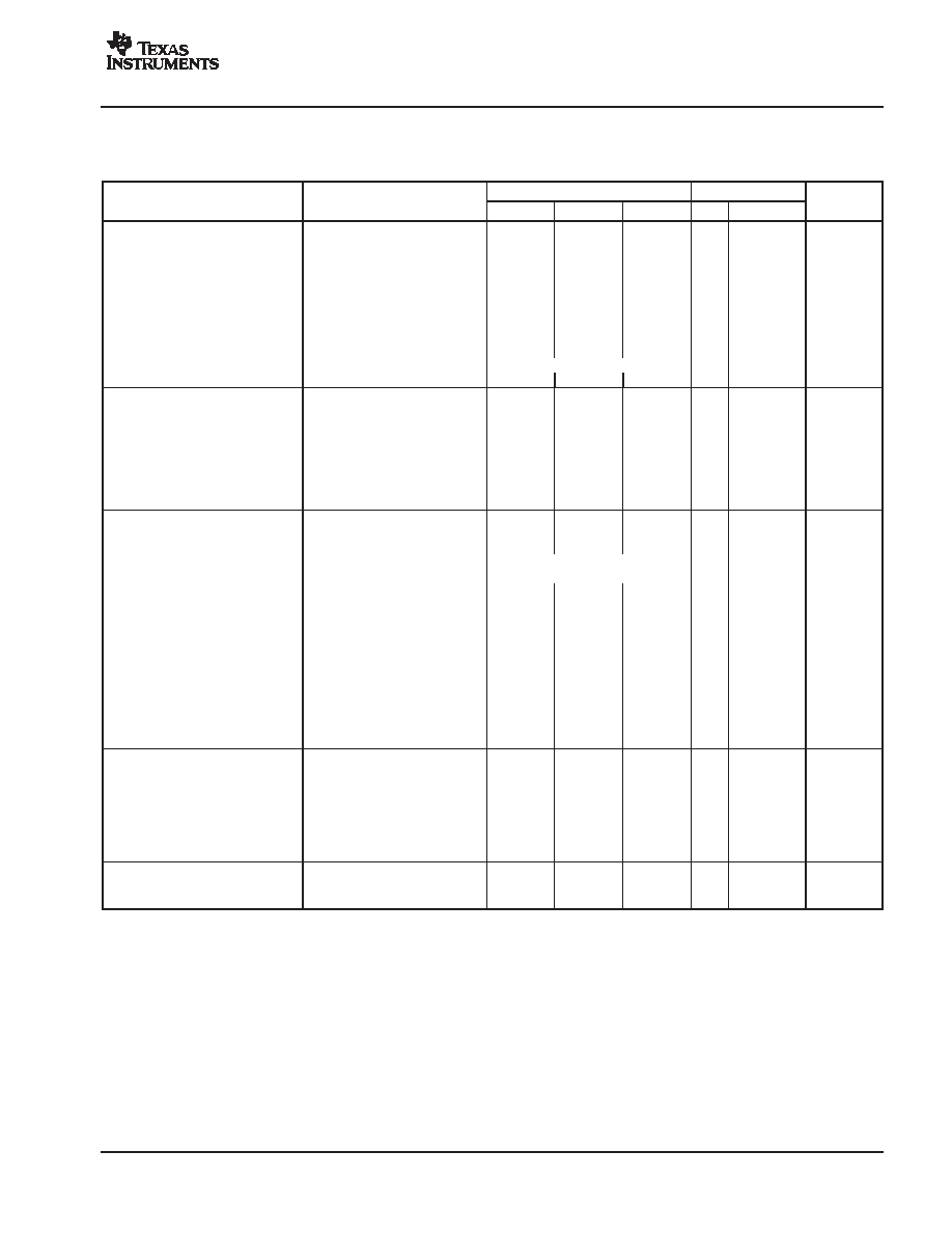
ELECTRICAL CHARACTERISTICS
At TA = +25°C, AVDD = +5V, DVDD = 3V, VREF = +4.096V, Range 5 (250pC), and continuous mode operation, unless otherwise noted.
Low-Power Mode: TINT = 400s and CLK = 4MHz; High-Speed Mode: TINT = 320s and CLK = 4.8MHz.
Low-Power Mode
High-Speed Mode
PARAMETER
TEST CONDITIONS
MIN
TYP
MAX
MIN
TYP
MAX
UNITS
ANALOG INPUT RANGE
Range 0
10.2
12
13.8
(1)
pC
Range 1
47.5
50
52.5
pC
Range 2
95
100
105
pC
Range 3
142.5
150
157.5
pC
Range 4
190
200
210
pC
Range 5
237.5
250
262.5
pC
Range 6
285
300
315
pC
Range 7
332.5
350
367.5
pC
Negative Full-Scale Range
0.4% of Positive Full-Scale Range
pC
Input Current(2)
750
A
DYNAMIC CHARACTERISTICS
Data Rate
2.5
3.125
kSPS
Integration Time, TINT
Continuous Mode
400
1,000,000
320
S
Integration Time, TINT
Non-continuous Mode, Range 1 to 7
50
S
System Clock Input (CLK)
CLK_4X = 0
4
4.8
MHz
CLK_4X = 1
16
19.2
MHz
Data Clock (DCLK)
16
MHz
ACCURACY
Noise, Low-Level Input(3)
CSENSOR(4) = 50pF, Range 5 (250pC)
5.2
6.5
5.5
7
ppm of
FSR(5), rms
Integral Linearity Error(6)
±0.01% Reading ± 0.5ppm FSR, typ
Integral Linearity Error(6)
±0.025% Reading ± 1.0ppm FSR, max
Resolution
FORMAT = 1
20
Bits
Resolution
FORMAT = 0
16
Bits
Input Bias Current
0.1
10
pA
Range Error Match(7)
All Ranges
0.1
0.5
% of FSR
Range Sensitivity to VREF
VREF = 4.096 ± 0.1V
1:1
Offset Error
Range 5 (250pC)
±400
±1000
ppm of FSR
Offset Error Match(7)
±100
ppm of FSR
DC Bias Voltage(9)
Low-Level Input (< 1% FSR)
±0.05
±2
mV
Power-Supply Rejection Ratio
at dc
±25
±200
ppm of FSR/V
Internal Test Signal
11
pC
Internal Test Accuracy
±10
%
PERFORMANCE OVER TEMPERATURE
Offset Drift
±0.5
±3(8)
ppm of
FSR/
°C
Offset Drift Stability
±0.2
±1(8)
ppm of FSR/
minute
DC Bias Voltage Drift(9)
3
V/°C
Input Bias Current Drift
TA = +25°C to +45°C
0.01
1(8)
pA/
°C
Range Drift(10)
25
ppm/
°C
REFERENCE
Voltage
4.000
4.096
4.200
V
Input Current(11)
Average Value
150
190
A
(1)
indicates that specification is the same as Low-Power Mode.
(2) Exceeding maximum input current specification may damage device.
(3) Input is less than 1% of full scale.
(4) CSENSOR is the capacitance seen at the DDC118 inputs from wiring, photodiode, etc.
(5) FSR is Full-Scale Range.
(6) A best-fit line is used in measuring nonlinearity.
(7) Matching between side A and side B of the same input.
(8) Ensured by design, not production tested.
(9) Voltage produced by the DDC118 at its input which is applied to the sensor.
(10)Range drift does not include external reference drift.
(11)Input reference current decreases with increasing TINT (see the Voltage Reference section, page 11).
(12)Data format is Straight Binary with a small offset. The number of bits in the output word is controlled by the FORMAT pin (see text).
相关PDF资料 |
PDF描述 |
|---|---|
| DPB25F0/25F | 50 CONTACT(S), FEMALE-FEMALE, D SUBMINIATURE CONNECTOR, SOLDER |
| DPB25M/25M0 | 50 CONTACT(S), MALE-MALE, D SUBMINIATURE CONNECTOR, SOLDER |
| DPB25M/25M | 50 CONTACT(S), MALE-MALE, D SUBMINIATURE CONNECTOR, SOLDER |
| DPB25M0/25M0 | 50 CONTACT(S), MALE-MALE, D SUBMINIATURE CONNECTOR, SOLDER |
| DPB25M0/25M | 50 CONTACT(S), MALE-MALE, D SUBMINIATURE CONNECTOR, SOLDER |
相关代理商/技术参数 |
参数描述 |
|---|---|
| DDC118IRTCT | 制造商:Texas Instruments 功能描述:IC ADC 20BIT OCTAL 48-VQFN |
| DDC118IRTCT | 制造商:Texas Instruments 功能描述:A/D CONVERTER (A-D) IC ((NW)) |
| DDC118IRTCTG4 | 功能描述:模数转换器 - ADC Octal Current-Input 20-Bit RoHS:否 制造商:Texas Instruments 通道数量:2 结构:Sigma-Delta 转换速率:125 SPs to 8 KSPs 分辨率:24 bit 输入类型:Differential 信噪比:107 dB 接口类型:SPI 工作电源电压:1.7 V to 3.6 V, 2.7 V to 5.25 V 最大工作温度:+ 85 C 安装风格:SMD/SMT 封装 / 箱体:VQFN-32 |
| DDC11XEVM-PDK | 功能描述:数据转换 IC 开发工具 DDC11xEVM-PDK Eval Mod RoHS:否 制造商:Texas Instruments 产品:Demonstration Kits 类型:ADC 工具用于评估:ADS130E08 接口类型:SPI 工作电源电压:- 6 V to + 6 V |
| DDC122LH | 制造商:DIODES 制造商全称:Diodes Incorporated 功能描述:NPN PRE-BIASED SMALL SIGNAL SOT-563 DUAL SURFACE MOUNT TRANSISTOR |
发布紧急采购,3分钟左右您将得到回复。