- 您现在的位置:买卖IC网 > PDF目录212189 > DDC118IRTCT (TEXAS INSTRUMENTS INC) 8-CH 20-BIT DELTA-SIGMA ADC, SERIAL ACCESS, PQCC48 PDF资料下载
参数资料
| 型号: | DDC118IRTCT |
| 厂商: | TEXAS INSTRUMENTS INC |
| 元件分类: | ADC |
| 英文描述: | 8-CH 20-BIT DELTA-SIGMA ADC, SERIAL ACCESS, PQCC48 |
| 封装: | GREEN, PLASTIC, QFN-48 |
| 文件页数: | 3/35页 |
| 文件大小: | 653K |
| 代理商: | DDC118IRTCT |
第1页第2页当前第3页第4页第5页第6页第7页第8页第9页第10页第11页第12页第13页第14页第15页第16页第17页第18页第19页第20页第21页第22页第23页第24页第25页第26页第27页第28页第29页第30页第31页第32页第33页第34页第35页
DDC118
SBAS325B JUNE 2004 REVISED APRIL 2009
www.ti.com
11
At the completion of an A/D conversion, the charge on the
integration capacitor (CF) is reset with SREF1 and SRESET
(see Figure 4 and Figure 5a). In this manner, the selected
capacitor is charged to the reference voltage, VREF. Once
the integration capacitor is charged, SREF1 and SRESET
are switched so that VREF is no longer connected to the
amplifier circuit while it waits to begin integrating (see
Figure 5b). With the rising edge of CONV, SINTA closes,
which begins the integration of side A. This process puts
the integrator stage into its integrate mode (see Figure 5c).
Charge from the input signal is collected on the integration
capacitor, causing the voltage output of the amplifier to
decrease. The falling edge of CONV stops the integration
by switching the input signal from side A to side B (SINTA
and SINTB). Prior to the falling edge of CONV, the signal on
side B was converted by the A/D converter and reset
during the time that side A was integrating. With the falling
edge of CONV, side B starts integrating the input signal.
Now the output voltage of the side A operational amplifier
is presented to the input of the
Σ A/D converter (see
Figure 5d).
Integration Capacitors
There are eight different capacitors available on-chip for
both sides of every channel in the DDC118. These internal
capacitors are trimmed in production to achieve the
specified performance for range error of the DDC118. The
range control pins (RANGE0-RANGE2) change the
capacitor value for all four integrators. Consequently, all
inputs and both sides of each input will always have the
same full-scale range. Table 1 shows the capacitor value
selected for each range selection.
Table 1. Range Selection of the DDC118
RANGE2
RANGE1
RANGE0
CF
(pF, typ)
INPUT RANGE
(pC, typ)
0
3
0.048 to 12
0
1
12.5
–0.2 to 50
0
1
0
25
–0.4 to 100
0
1
37.5
–0.6 to 150
1
0
50
–0.8 to 200
1
0
1
62.5
–0.1 to 250
1
0
75
–1.2 to 300
1
87.5
–1.4 to 350
Voltage Reference
The external voltage reference is used to reset the
integration capacitors before an integration cycle begins.
It is also used by the
Σ converter while the converter is
measuring the voltage stored on the integrators after an
integration cycle ends. During this sampling, the external
reference must supply the charge needed by the
Σ
converter. For an integration time of 400
s, this charge
translates to an average VREF current of approximately
150
A. The amount of charge needed by the Σ converter
is
independent of the integration time; therefore,
increasing the integration time lowers the average current.
For example, an integration time of 800
s lowers the
average VREF current to 75
A.
It is critical that VREF be stable during the different modes
of operation (see Figure 5). The
Σ converter measures
the voltage on the integrator with respect to VREF. Since
the integrator capacitors are initially reset to VREF, any
drop in VREF from the time the capacitors are reset to the
time when the converter measures the integrator output
will introduce an offset. It is also important that VREF be
stable over longer periods of time because changes in
VREF correspond directly to changes in the full-scale
range. Finally, VREF should introduce as little additional
noise as possible.
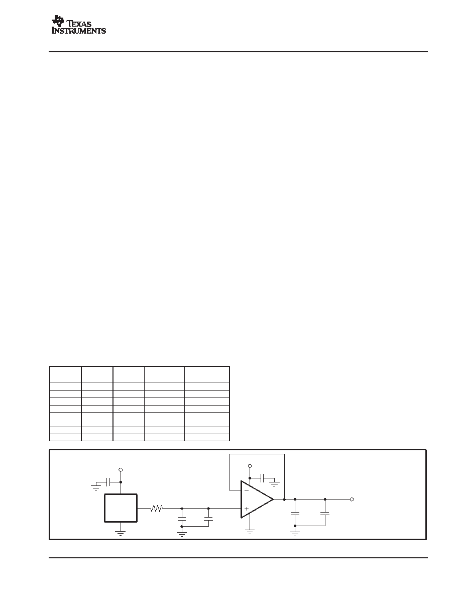
For these reasons, it is strongly recommended that the
external reference source be buffered with an operational
amplifier, as shown in Figure 6. In this circuit, the voltage
reference is generated by a 4.096V reference. A low-pass
filter to reduce noise connects the reference to an
operational amplifier configured as a buffer. This amplifier
should have low noise, and input/output common-mode
ranges that support VREF. Following the buffer are
capacitors placed close to the DDC118 VREF pin. Even
though the circuit in Figure 6 might appear to be unstable
because of the large output capacitors, it works well for
most operational amplifiers. It is NOT recommended that
series resistance be placed in the output lead to improve
stability since this can cause a drop in VREF, which
producing large offsets.
0.10
F
+5V
10k
10
F
4
3
2
3
1
2
7
6
+
0.10
F
0.1
F
10
F
+
OPA350
0.47
F
+5V
To VREF
Pin10of
the DDC118
REF3140
Figure 6. Recommended External Voltage Reference Circuit for Best Low-Noise Operation with the DDC118
相关PDF资料 |
PDF描述 |
|---|---|
| DPB25F0/25F | 50 CONTACT(S), FEMALE-FEMALE, D SUBMINIATURE CONNECTOR, SOLDER |
| DPB25M/25M0 | 50 CONTACT(S), MALE-MALE, D SUBMINIATURE CONNECTOR, SOLDER |
| DPB25M/25M | 50 CONTACT(S), MALE-MALE, D SUBMINIATURE CONNECTOR, SOLDER |
| DPB25M0/25M0 | 50 CONTACT(S), MALE-MALE, D SUBMINIATURE CONNECTOR, SOLDER |
| DPB25M0/25M | 50 CONTACT(S), MALE-MALE, D SUBMINIATURE CONNECTOR, SOLDER |
相关代理商/技术参数 |
参数描述 |
|---|---|
| DDC118IRTCT | 制造商:Texas Instruments 功能描述:IC ADC 20BIT OCTAL 48-VQFN |
| DDC118IRTCT | 制造商:Texas Instruments 功能描述:A/D CONVERTER (A-D) IC ((NW)) |
| DDC118IRTCTG4 | 功能描述:模数转换器 - ADC Octal Current-Input 20-Bit RoHS:否 制造商:Texas Instruments 通道数量:2 结构:Sigma-Delta 转换速率:125 SPs to 8 KSPs 分辨率:24 bit 输入类型:Differential 信噪比:107 dB 接口类型:SPI 工作电源电压:1.7 V to 3.6 V, 2.7 V to 5.25 V 最大工作温度:+ 85 C 安装风格:SMD/SMT 封装 / 箱体:VQFN-32 |
| DDC11XEVM-PDK | 功能描述:数据转换 IC 开发工具 DDC11xEVM-PDK Eval Mod RoHS:否 制造商:Texas Instruments 产品:Demonstration Kits 类型:ADC 工具用于评估:ADS130E08 接口类型:SPI 工作电源电压:- 6 V to + 6 V |
| DDC122LH | 制造商:DIODES 制造商全称:Diodes Incorporated 功能描述:NPN PRE-BIASED SMALL SIGNAL SOT-563 DUAL SURFACE MOUNT TRANSISTOR |
发布紧急采购,3分钟左右您将得到回复。