- 您现在的位置:买卖IC网 > PDF目录17120 > DK-DEV-2AGX125N (Altera)KIT DEV ARRIA II GX FPGA 2AGX125 PDF资料下载
参数资料
| 型号: | DK-DEV-2AGX125N |
| 厂商: | Altera |
| 文件页数: | 6/90页 |
| 文件大小: | 0K |
| 描述: | KIT DEV ARRIA II GX FPGA 2AGX125 |
| 产品培训模块: | Arria II GX FPGA Three Reasons to Use FPGA's in Industrial Designs |
| 特色产品: | Arria? II GX FPGA Development Kit |
| 标准包装: | 1 |
| 系列: | Arria II GX |
| 类型: | FPGA |
| 适用于相关产品: | EP2AGX125EF35 |
| 所含物品: | 板,线缆,CD,DVD,电源 |
| 产品目录页面: | 605 (CN2011-ZH PDF) |
| 相关产品: | 544-2599-5-ND - IC ARRIA II GX 125K 1152FBG 544-2598-5-ND - IC ARRIA II GX 125K 1152FBG 544-2597-5-ND - IC ARRIA II GX 125K 1152FBG |
| 其它名称: | 544-2600 |
第1页第2页第3页第4页第5页当前第6页第7页第8页第9页第10页第11页第12页第13页第14页第15页第16页第17页第18页第19页第20页第21页第22页第23页第24页第25页第26页第27页第28页第29页第30页第31页第32页第33页第34页第35页第36页第37页第38页第39页第40页第41页第42页第43页第44页第45页第46页第47页第48页第49页第50页第51页第52页第53页第54页第55页第56页第57页第58页第59页第60页第61页第62页第63页第64页第65页第66页第67页第68页第69页第70页第71页第72页第73页第74页第75页第76页第77页第78页第79页第80页第81页第82页第83页第84页第85页第86页第87页第88页第89页第90页
1–6
Chapter 1: Device Datasheet for Arria II Devices
Electrical Characteristics
December 2013
Altera Corporation
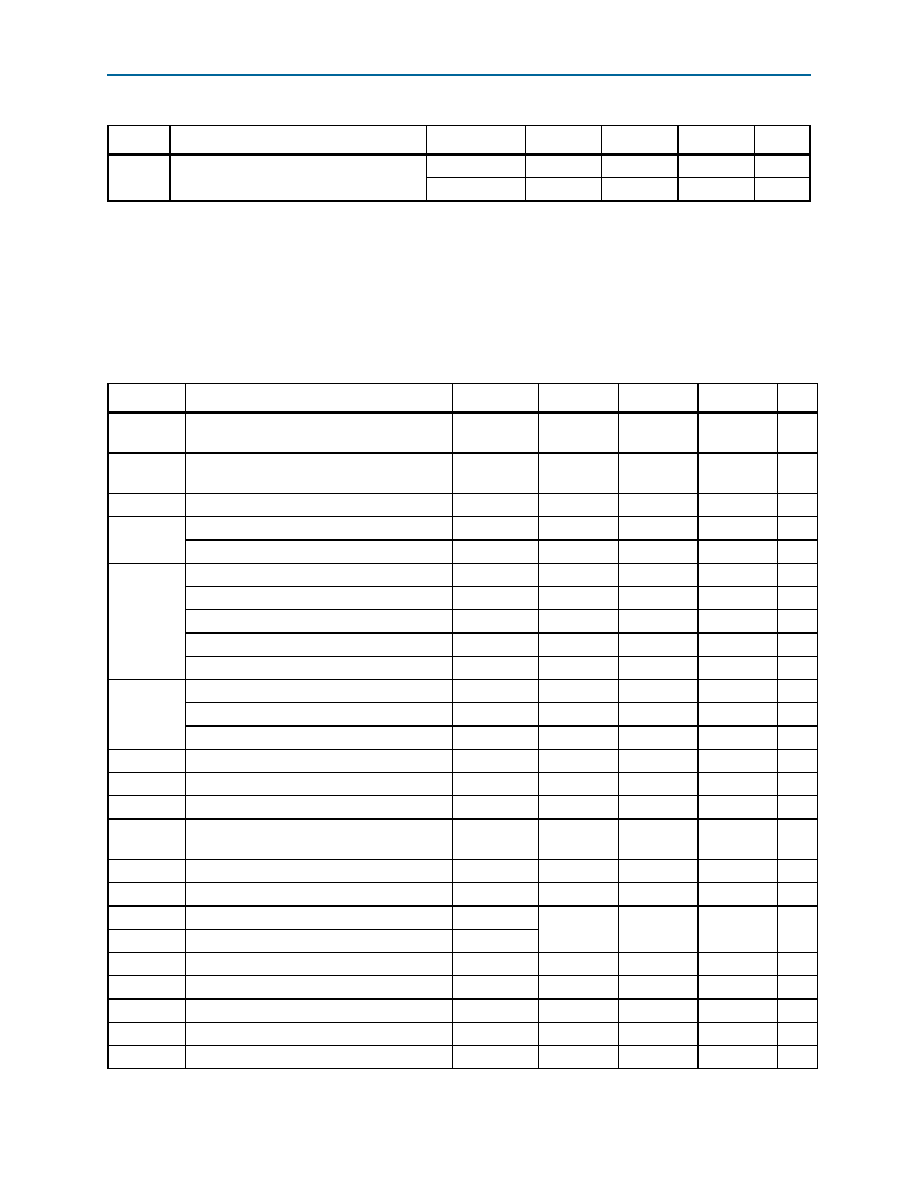
Table 1–6 lists the recommended operating conditions for Arria II GZ devices.
tRAMP
Power Supply Ramp time
Normal POR
0.05
—
100
ms
Fast POR
0.05
—
4
ms
Notes to Table 1–5:
(1) For more information about supply pin connections, refer to the Arria II Device Family Pin Connection Guidelines.
(2) Altera recommends a 3.0-V nominal battery voltage when connecting VCCBAT to a battery for volatile key backup. If you do not use the volatile
security key, you may connect the VCCBAT to either GND or a 3.0-V power supply.
(3) VCCPD must be 2.5-V for I/O banks with 2.5-V and lower VCCIO, 3.0-V for 3.0-V VCCIO, and 3.3-V for 3.3-V VCCIO.
(4) VCCIO for 3C and 8C I/O banks where the configuration pins reside only supports 3.3-, 3.0-, 2.5-, or 1.8-V voltage levels.
Table 1–5. Recommended Operating Conditions for Arria II GX Devices (Note 1) (Part 2 of 2)
Symbol
Description
Condition
Minimum
Typical
Maximum
Unit
Table 1–6. Recommended Operating Conditions for Arria II GZ Devices (Note 6) (Part 1 of 2)
Symbol
Description
Condition
Minimum
Typical
Maximum
Unit
VCC
Core voltage and periphery circuitry power
supply
—
0.87
0.90
0.93
V
VCCCB
Supplies power for the configuration RAM
bits
—
1.45
1.50
1.55
V
VCCAUX
Auxiliary supply
—
2.375
2.5
2.625
V
VCCPD (2)
I/O pre-driver (3.0 V) power supply
—
2.85
3.0
3.15
V
I/O pre-driver (2.5 V) power supply
—
2.375
2.5
2.625
V
VCCIO
I/O buffers (3.0 V) power supply
—
2.85
3.0
3.15
V
I/O buffers (2.5 V) power supply
—
2.375
2.5
2.625
V
I/O buffers (1.8 V) power supply
—
1.71
1.8
1.89
V
I/O buffers (1.5 V) power supply
—
1.425
1.5
1.575
V
I/O buffers (1.2 V) power supply
—
1.14
1.2
1.26
V
VCCPGM
Configuration pins (3.0 V) power supply
—
2.85
3.0
3.15
V
Configuration pins (2.5 V) power supply
—
2.375
2.5
2.625
V
Configuration pins (1.8 V) power supply
—
1.71
1.8
1.89
V
VCCA_PLL
PLL analog voltage regulator power supply
—
2.375
2.5
2.625
V
VCCD_PLL
PLL digital voltage regulator power supply
—
0.87
0.90
0.93
V
VCC_CLKIN
Differential clock input power supply
—
2.375
2.5
2.625
V
VCCBAT (1)
Battery back-up power supply (For design
security volatile key register)
—
1.2—3.3
V
VI
DC input voltage
—
–0.5
—
3.6
V
VO
Output voltage
—
0
—
VCCIO
V
VCCA_L
Transceiver high voltage power (left side)
—
2.85/2.375
3.0/2.5 (4)
3.15/2.625
V
VCCA_R
Transceiver high voltage power (right side)
—
VCCHIP_L
Transceiver HIP digital power (left side)
—
0.87
0.9
0.93
V
VCCR_L
Receiver power (left side)
—
1.05
1.1
1.15
V
VCCR_R
Receiver power (right side)
—
1.05
1.1
1.15
V
VCCT_L
Transmitter power (left side)
—
1.05
1.1
1.15
V
VCCT_R
Transmitter power (right side)
—
1.05
1.1
1.15
V
相关PDF资料 |
PDF描述 |
|---|---|
| DK-V6-EMBD-G-J | DEV KIT EMBEDDED VIRTEX 6 |
| VE-J5V-EZ | CONVERTER MOD DC/DC 5.8V 25W |
| AP432AL-13 | IC VREF SHUNT PREC ADJ 8-SOP |
| GCC18DRTH-S13 | CONN EDGECARD 36POS .100 EXTEND |
| RCM15DRXS | CONN EDGECARD 30POS DIP .156 SLD |
相关代理商/技术参数 |
参数描述 |
|---|---|
| DK-DEV-2AGX260N | 功能描述:可编程逻辑 IC 开发工具 FPGA Development Kit For EP2AGX260 RoHS:否 制造商:Altera Corporation 产品:Development Kits 类型:FPGA 工具用于评估:5CEFA7F3 接口类型: 工作电源电压: |
| DK-DEV-3C120N | 功能描述:可编程逻辑 IC 开发工具 FPGA Development Kit For EP3C120F780 RoHS:否 制造商:Altera Corporation 产品:Development Kits 类型:FPGA 工具用于评估:5CEFA7F3 接口类型: 工作电源电压: |
| DK-DEV-3CLS200N | 功能描述:可编程逻辑 IC 开发工具 FPGA Development Kit For EP3CLS200F780 RoHS:否 制造商:Altera Corporation 产品:Development Kits 类型:FPGA 工具用于评估:5CEFA7F3 接口类型: 工作电源电压: |
| DK-DEV-3SL150N | 功能描述:可编程逻辑 IC 开发工具 FPGA Development Kit For EP3SL150F152 RoHS:否 制造商:Altera Corporation 产品:Development Kits 类型:FPGA 工具用于评估:5CEFA7F3 接口类型: 工作电源电压: |
| DK-DEV-3SL150N/ES | 制造商:Altera Corporation 功能描述:KIT DEVELOPMENT STRATIX II ES |
发布紧急采购,3分钟左右您将得到回复。