- 您现在的位置:买卖IC网 > PDF目录17120 > DK-DEV-2AGX125N (Altera)KIT DEV ARRIA II GX FPGA 2AGX125 PDF资料下载
参数资料
| 型号: | DK-DEV-2AGX125N |
| 厂商: | Altera |
| 文件页数: | 79/90页 |
| 文件大小: | 0K |
| 描述: | KIT DEV ARRIA II GX FPGA 2AGX125 |
| 产品培训模块: | Arria II GX FPGA Three Reasons to Use FPGA's in Industrial Designs |
| 特色产品: | Arria? II GX FPGA Development Kit |
| 标准包装: | 1 |
| 系列: | Arria II GX |
| 类型: | FPGA |
| 适用于相关产品: | EP2AGX125EF35 |
| 所含物品: | 板,线缆,CD,DVD,电源 |
| 产品目录页面: | 605 (CN2011-ZH PDF) |
| 相关产品: | 544-2599-5-ND - IC ARRIA II GX 125K 1152FBG 544-2598-5-ND - IC ARRIA II GX 125K 1152FBG 544-2597-5-ND - IC ARRIA II GX 125K 1152FBG |
| 其它名称: | 544-2600 |
第1页第2页第3页第4页第5页第6页第7页第8页第9页第10页第11页第12页第13页第14页第15页第16页第17页第18页第19页第20页第21页第22页第23页第24页第25页第26页第27页第28页第29页第30页第31页第32页第33页第34页第35页第36页第37页第38页第39页第40页第41页第42页第43页第44页第45页第46页第47页第48页第49页第50页第51页第52页第53页第54页第55页第56页第57页第58页第59页第60页第61页第62页第63页第64页第65页第66页第67页第68页第69页第70页第71页第72页第73页第74页第75页第76页第77页第78页当前第79页第80页第81页第82页第83页第84页第85页第86页第87页第88页第89页第90页
1–72
Chapter 1: Device Datasheet for Arria II Devices
Switching Characteristics
December 2013
Altera Corporation
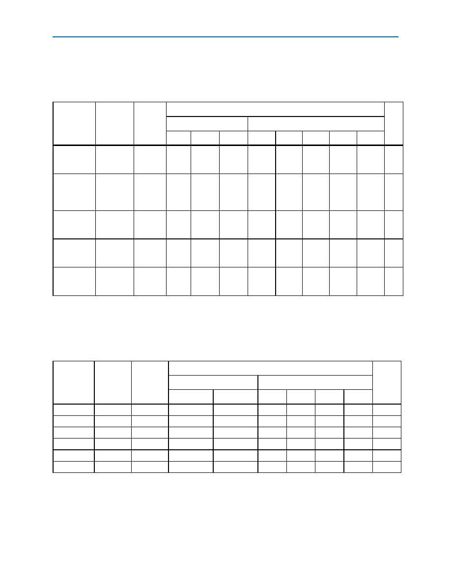
IOE Programmable Delay
Table 1–66 lists the delay associated with each supported IOE programmable delay
chain for Arria II GX devices.
Table 1–67 lists the IOE programmable delay settings for Arria II GZ devices.
Table 1–66. IOE Programmable Delay for Arria II GX Devices
Parameter
Available
Settings
Minimum
Offset
Maximum Offset
Unit
Fast Model
Slow Model
I3
C4
I5
I3
C4
C5
I5
C6
Output
enable pin
delay
7
0
0.413
0.442
0.413
0.814
0.713
0.796
0.801
0.873
ns
Delay from
output
register to
output pin
7
0
0.339
0.362
0.339
0.671
0.585
0.654
0.661
0.722
ns
Input delay
from pin to
internal cell
52
0
1.494
1.607
1.494
2.895
2.520
2.733
2.775
2.944
ns
Input delay
from pin to
input register
52
0
1.493
1.607
1.493
2.896
2.503
2.732
2.774
2.944
ns
DQS bus to
input register
delay
4
0
0.074
0.076
0.074
0.140
0.124
0.147
0.167
ns
Notes to Table 1–66:
(1) The available setting for every delay chain starts with zero and ends with the specified maximum number of settings.
(2) The minimum offset represented in the table does not include intrinsic delay.
Table 1–67. IOE Programmable Delay for Arria II GZ Devices
Parameter
Available
Settings
Minimum
Offset (2)
Maximum Offset
Unit
Fast Model
Slow Model
Industrial
Commercial
C3
I3
C4
I4
D1
15
0
0.462
0.505
0.795
0.801
0.857
0.864
ns
D2
7
0
0.234
0.232
0.372
0.371
0.407
0.405
ns
D3
7
0
1.700
1.769
2.927
2.948
3.157
3.178
ns
D4
15
0
0.508
0.554
0.882
0.889
0.952
0.959
ns
D5
15
0
0.472
0.500
0.799
0.817
0.875
0.882
ns
D6
6
0
0.186
0.195
0.319
0.321
0.345
0.347
ns
Notes to Table 1–67:
(1) You can set this value in the Quartus II software by selecting D1, D2, D3, D4, D5, and D6 in the Assignment Name column.
(2) Minimum offset does not include the intrinsic delay.
相关PDF资料 |
PDF描述 |
|---|---|
| DK-V6-EMBD-G-J | DEV KIT EMBEDDED VIRTEX 6 |
| VE-J5V-EZ | CONVERTER MOD DC/DC 5.8V 25W |
| AP432AL-13 | IC VREF SHUNT PREC ADJ 8-SOP |
| GCC18DRTH-S13 | CONN EDGECARD 36POS .100 EXTEND |
| RCM15DRXS | CONN EDGECARD 30POS DIP .156 SLD |
相关代理商/技术参数 |
参数描述 |
|---|---|
| DK-DEV-2AGX260N | 功能描述:可编程逻辑 IC 开发工具 FPGA Development Kit For EP2AGX260 RoHS:否 制造商:Altera Corporation 产品:Development Kits 类型:FPGA 工具用于评估:5CEFA7F3 接口类型: 工作电源电压: |
| DK-DEV-3C120N | 功能描述:可编程逻辑 IC 开发工具 FPGA Development Kit For EP3C120F780 RoHS:否 制造商:Altera Corporation 产品:Development Kits 类型:FPGA 工具用于评估:5CEFA7F3 接口类型: 工作电源电压: |
| DK-DEV-3CLS200N | 功能描述:可编程逻辑 IC 开发工具 FPGA Development Kit For EP3CLS200F780 RoHS:否 制造商:Altera Corporation 产品:Development Kits 类型:FPGA 工具用于评估:5CEFA7F3 接口类型: 工作电源电压: |
| DK-DEV-3SL150N | 功能描述:可编程逻辑 IC 开发工具 FPGA Development Kit For EP3SL150F152 RoHS:否 制造商:Altera Corporation 产品:Development Kits 类型:FPGA 工具用于评估:5CEFA7F3 接口类型: 工作电源电压: |
| DK-DEV-3SL150N/ES | 制造商:Altera Corporation 功能描述:KIT DEVELOPMENT STRATIX II ES |
发布紧急采购,3分钟左右您将得到回复。