- 您现在的位置:买卖IC网 > PDF目录17120 > DK-DEV-2AGX125N (Altera)KIT DEV ARRIA II GX FPGA 2AGX125 PDF资料下载
参数资料
| 型号: | DK-DEV-2AGX125N |
| 厂商: | Altera |
| 文件页数: | 64/90页 |
| 文件大小: | 0K |
| 描述: | KIT DEV ARRIA II GX FPGA 2AGX125 |
| 产品培训模块: | Arria II GX FPGA Three Reasons to Use FPGA's in Industrial Designs |
| 特色产品: | Arria? II GX FPGA Development Kit |
| 标准包装: | 1 |
| 系列: | Arria II GX |
| 类型: | FPGA |
| 适用于相关产品: | EP2AGX125EF35 |
| 所含物品: | 板,线缆,CD,DVD,电源 |
| 产品目录页面: | 605 (CN2011-ZH PDF) |
| 相关产品: | 544-2599-5-ND - IC ARRIA II GX 125K 1152FBG 544-2598-5-ND - IC ARRIA II GX 125K 1152FBG 544-2597-5-ND - IC ARRIA II GX 125K 1152FBG |
| 其它名称: | 544-2600 |
第1页第2页第3页第4页第5页第6页第7页第8页第9页第10页第11页第12页第13页第14页第15页第16页第17页第18页第19页第20页第21页第22页第23页第24页第25页第26页第27页第28页第29页第30页第31页第32页第33页第34页第35页第36页第37页第38页第39页第40页第41页第42页第43页第44页第45页第46页第47页第48页第49页第50页第51页第52页第53页第54页第55页第56页第57页第58页第59页第60页第61页第62页第63页当前第64页第65页第66页第67页第68页第69页第70页第71页第72页第73页第74页第75页第76页第77页第78页第79页第80页第81页第82页第83页第84页第85页第86页第87页第88页第89页第90页
Chapter 1: Device Datasheet for Arria II Devices
1–59
Switching Characteristics
December 2013
Altera Corporation
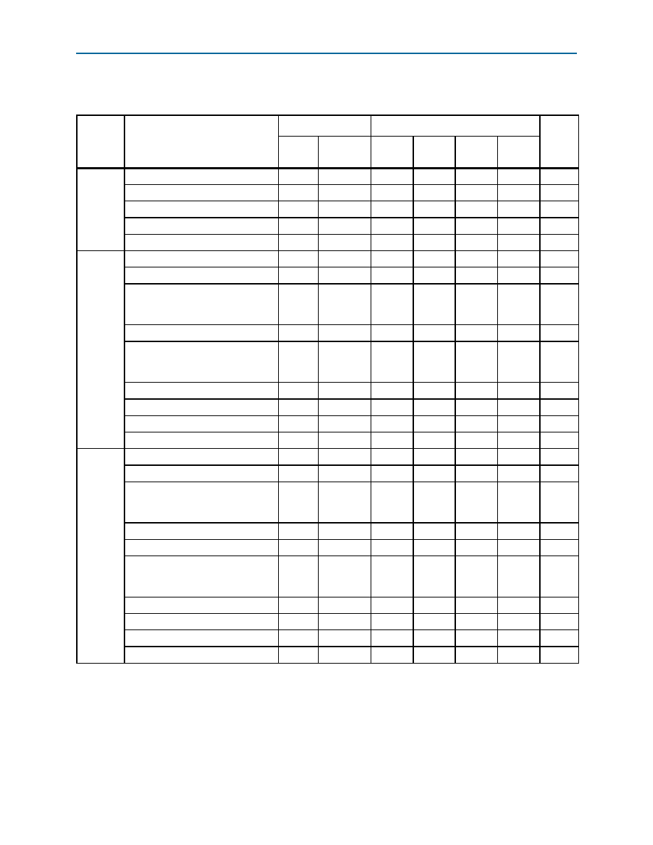
Table 1–49 lists the embedded memory block specifications for Arria II GZ devices.
Table 1–49. Embedded Memory Block Performance Specifications for Arria II GZ Devices (Note 1)
Memory
Mode
Resources Used
Performance
Unit
ALUTs
TriMatrix
Memory
C3
I3
C4
I4
MLAB
Single port 64 × 10
0
1
500
450
MHz
Simple dual-port 32 × 20
0
1
500
450
MHz
Simple dual-port 64 × 10
0
1
500
450
MHz
ROM 64 × 10
0
1
500
450
MHz
ROM 32 × 20
0
1
500
450
MHz
M9K
Block (2)
Single-port 256 × 36
0
1
540
475
MHz
Simple dual-port 256 × 36
0
1
490
420
MHz
Simple dual-port 256 × 36, with the
read-during-write option set to Old
Data
0
1
340
300
MHz
True dual port 512 × 18
0
1
430
370
MHz
True dual-port 512 × 18, with the
read-during-write option set to Old
Data
0
1
335
290
MHz
ROM 1 Port
0
1
540
475
MHz
ROM 2 Port
0
1
540
475
MHz
Min Pulse Width (clock high time)
—
800
850
ps
Min Pulse Width (clock low time)
—
625
690
ps
M144K
Block (2)
Single-port 2K × 72
0
1
440
400
380
350
MHz
Simple dual-port 2K × 72
0
1
435
375
385
325
MHz
Simple dual-port 2K × 72, with the
read-during-write option set to Old
Data
0
1
240
225
205
200
MHz
Simple dual-port 2K × 64 (with ECC)
0
1
300
295
255
250
MHz
True dual-port 4K × 36
0
1
375
350
330
310
MHz
True dual-port 4K × 36, with the
read-during-write option set to Old
Data
0
1
230
225
205
200
MHz
ROM 1 Port
0
1
500
450
435
420
MHz
ROM 2 Port
0
1
465
425
400
MHz
Min Pulse Width (clock high time)
—
755
860
950
ps
Min Pulse Width (clock low time)
—
625
690
ps
Notes to Table 1–48:
(1) To achieve the maximum memory block performance, use a memory block clock that comes through global clock routing from an on-chip PLL
set to 50% output duty cycle. Use the Quartus II software to report timing for this and other memory block clocking schemes.
(2) When you use the error detection CRC feature, there is no degradation in FMAX.
相关PDF资料 |
PDF描述 |
|---|---|
| DK-V6-EMBD-G-J | DEV KIT EMBEDDED VIRTEX 6 |
| VE-J5V-EZ | CONVERTER MOD DC/DC 5.8V 25W |
| AP432AL-13 | IC VREF SHUNT PREC ADJ 8-SOP |
| GCC18DRTH-S13 | CONN EDGECARD 36POS .100 EXTEND |
| RCM15DRXS | CONN EDGECARD 30POS DIP .156 SLD |
相关代理商/技术参数 |
参数描述 |
|---|---|
| DK-DEV-2AGX260N | 功能描述:可编程逻辑 IC 开发工具 FPGA Development Kit For EP2AGX260 RoHS:否 制造商:Altera Corporation 产品:Development Kits 类型:FPGA 工具用于评估:5CEFA7F3 接口类型: 工作电源电压: |
| DK-DEV-3C120N | 功能描述:可编程逻辑 IC 开发工具 FPGA Development Kit For EP3C120F780 RoHS:否 制造商:Altera Corporation 产品:Development Kits 类型:FPGA 工具用于评估:5CEFA7F3 接口类型: 工作电源电压: |
| DK-DEV-3CLS200N | 功能描述:可编程逻辑 IC 开发工具 FPGA Development Kit For EP3CLS200F780 RoHS:否 制造商:Altera Corporation 产品:Development Kits 类型:FPGA 工具用于评估:5CEFA7F3 接口类型: 工作电源电压: |
| DK-DEV-3SL150N | 功能描述:可编程逻辑 IC 开发工具 FPGA Development Kit For EP3SL150F152 RoHS:否 制造商:Altera Corporation 产品:Development Kits 类型:FPGA 工具用于评估:5CEFA7F3 接口类型: 工作电源电压: |
| DK-DEV-3SL150N/ES | 制造商:Altera Corporation 功能描述:KIT DEVELOPMENT STRATIX II ES |
发布紧急采购,3分钟左右您将得到回复。