- 您现在的位置:买卖IC网 > PDF目录16258 > DS3254DK (Maxim Integrated Products)KIT DEMO FOR DS3254 PDF资料下载
参数资料
| 型号: | DS3254DK |
| 厂商: | Maxim Integrated Products |
| 文件页数: | 3/71页 |
| 文件大小: | 0K |
| 描述: | KIT DEMO FOR DS3254 |
| 产品培训模块: | Lead (SnPb) Finish for COTS Obsolescence Mitigation Program |
| 设计资源: | DS3254DK Gerber Files |
| 标准包装: | 1 |
| 主要目的: | 电信,线路接口单元(LIU) |
| 已用 IC / 零件: | DS3254 |
| 已供物品: | 板,CD |
第1页第2页当前第3页第4页第5页第6页第7页第8页第9页第10页第11页第12页第13页第14页第15页第16页第17页第18页第19页第20页第21页第22页第23页第24页第25页第26页第27页第28页第29页第30页第31页第32页第33页第34页第35页第36页第37页第38页第39页第40页第41页第42页第43页第44页第45页第46页第47页第48页第49页第50页第51页第52页第53页第54页第55页第56页第57页第58页第59页第60页第61页第62页第63页第64页第65页第66页第67页第68页第69页第70页第71页
DS3251/DS3252/DS3253/DS3254
11 of 71
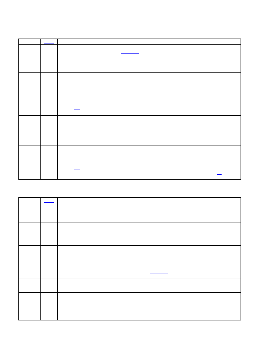
Table 6-B. Receiver Pin Descriptions
Note: These pins are always active.
NAME
FUNCTION
RXPn,
RXNn
I
Receiver Analog Inputs. These differential AMI inputs are coupled to the inbound 75
coaxial cable
through a 1:2 step-up transformer (Figure 2-1).
RCLKn
O3
Receiver Clock. The recovered clock is output on the RCLK pin. Recovered data is output on the
RPOS/RDAT and RNEG/RLCV pins on the falling edge of RCLK (RCINV = 0) or the rising edge of
RCLK (RCINV = 1). During a loss of signal (
RLOS = 0), the RCLK output signal is derived from the
LIU’s master clock.
RPOSn/
RDATn
O3
Receiver Positive AMI/Receiver Data. When the receiver is configured to have a bipolar interface
(RBIN = 0), RPOS pulses high for each positive AMI pulse received. When the receiver is configured
to have a binary interface (RBIN = 1), RDAT outputs decoded binary data. RPOS/RDAT is updated
either on the falling edge of RCLK (RCINV = 0) or the rising edge of RCLK (RCINV = 1).
RNEGn/
RLCVn
O3
Receiver Negative AMI/Line-Code Violation. When the receiver is configured to have a bipolar
interface (RBIN = 0), RNEG pulses high for each negative AMI pulse received. When the receiver is
configured to have a binary interface (RBIN = 1), RLCV pulses high to flag code violations. See
Section 8.6 for further details on code violations. RNEG/RLCV is updated either on the falling edge of
RCLK (RCINV = 0) or the rising edge of RCLK (RCINV = 1).
RTSn
I
Receiver Tri-State Enable (Active Low).
RTS tri-states the RPOS/RDAT, RNEG/RLCV, and RCLK
receiver outputs. This feature supports applications requiring LIU redundancy. Receiver outputs from
multiple LIUs can be wire-ORed together, eliminating the need for external switches or muxes. The
receiver continues to operate internally when
RTS is low.
0 = tri-state the receiver outputs
1 = enable the receiver outputs
RLOSn
O
Receiver Loss of Signal (Active Low, Open Drain).
RLOS is asserted upon detection of 175
±75
consecutive zeros in the receive data stream.
RLOS is deasserted when there are no excessive zero
occurrences over a span of 175
±75 clock periods. An excessive zero occurrence is defined as three
or more consecutive zeros in the DS3 and STS-1 modes or four or more zeros in the E3 mode. See
Section 8.5 for more information.
PRBSn
O
PRBS Detector Output. This signal reports the status of the PRBS detector. See Section 11 for
further details.
Table 6-C. Transmitter Pin Descriptions
Note: These pins are always active.
NAME
FUNCTION
TCLKn
I
Transmitter Clock. A DS3 (44.736MHz
±20ppm), E3 (34.368MHz ±20ppm), or STS-1 (51.840MHz
±20ppm) clock should be applied at this signal. Data to be transmitted is clocked into the device at
TPOS/TDAT and TNEG either on the rising edge of TCLK (TCINV = 0) or the falling edge of TCLK
(TCINV = 1). See Section 9 for additional details.
TPOSn/
TDATn
I
Transmitter Positive AMI/Transmitter Data. When the transmitter is configured to have a bipolar
interface (TBIN = 0), a positive pulse is transmitted on the line when TPOS is high. When the
transmitter is configured to have a binary interface (TBIN = 1), the data on TDAT is transmitted after
B3ZS or HDB3 encoding. TPOS/TDAT is sampled either on the rising edge of TCLK (TCINV = 0) or
on the falling edge of TCLK (TCINV = 1).
TNEGn
I
Transmitter Negative AMI. When the transmitter is configured to have a bipolar interface (TBIN = 0),
a negative pulse is transmitted on the line when TNEG is high. When the transmitter is configured to
have a binary interface (TBIN = 1), TNEG is ignored and should be wired either high or low. TNEG is
sampled either on the rising edge of TCLK (TCINV = 0) or on the falling edge of TCLK (TCINV = 1).
TXPn,
TXNn
O3
Transmitter Analog Outputs. These differential AMI outputs are coupled to the outbound 75
coaxial cable through a 2:1 step-down transformer (Figure 2-1). These outputs can be tri-stated using
the
TTS pin or the TTS or TPS configuration bits.
TDMn
O
Transmitter Driver Monitor (Active Low, Open Drain).
TDM reports the status of the transmit driver
monitor. When the monitor detects a faulty transmitter,
TDM is driven low. TDM requires an external
TTSn
I
Transmitter Tri-State Enable (Active Low).
TTS tri-states the transmitter outputs (TXP and TXN).
This feature supports applications requiring LIU redundancy. Transmitter outputs from multiple LIUs
can be wire-ORed together, eliminating external switches. The transmitter continues to operate
internally when
TTS is active.
0 = tri-state the transmitter output driver
1 = enable the transmitter output driver
相关PDF资料 |
PDF描述 |
|---|---|
| GCA32DRMH-S288 | CONN EDGECARD 64POS .125 EXTEND |
| EET-UQ2G471CA | CAP ALUM 470UF 400V 20% SNAP |
| UCY2G680MHD | CAP ALUM 68UF 400V 20% RADIAL |
| RCC22DCMS | CONN EDGECARD 44POS .100 WW |
| VE-JWK-EY-S | CONVERTER MOD DC/DC 40V 50W |
相关代理商/技术参数 |
参数描述 |
|---|---|
| DS3254N | 功能描述:网络控制器与处理器 IC Quad DS3/E3/STS-1 Line Interface Unit RoHS:否 制造商:Micrel 产品:Controller Area Network (CAN) 收发器数量: 数据速率: 电源电流(最大值):595 mA 最大工作温度:+ 85 C 安装风格:SMD/SMT 封装 / 箱体:PBGA-400 封装:Tray |
| DS3254N# | 功能描述:网络控制器与处理器 IC Quad DS3/E3/STS-1 Line Interface Unit RoHS:否 制造商:Micrel 产品:Controller Area Network (CAN) 收发器数量: 数据速率: 电源电流(最大值):595 mA 最大工作温度:+ 85 C 安装风格:SMD/SMT 封装 / 箱体:PBGA-400 封装:Tray |
| DS3254N+ | 功能描述:网络控制器与处理器 IC Quad DS3/E3/STS-1 Line Interface Unit RoHS:否 制造商:Micrel 产品:Controller Area Network (CAN) 收发器数量: 数据速率: 电源电流(最大值):595 mA 最大工作温度:+ 85 C 安装风格:SMD/SMT 封装 / 箱体:PBGA-400 封装:Tray |
| DS3254NA3 | 制造商:Maxim Integrated Products 功能描述:QUAD ENH DS3/E3 LIU REV A3 IND - Rail/Tube |
| DS3256 | 功能描述:网络控制器与处理器 IC X6 T3/E3 Line Interface Unit RoHS:否 制造商:Micrel 产品:Controller Area Network (CAN) 收发器数量: 数据速率: 电源电流(最大值):595 mA 最大工作温度:+ 85 C 安装风格:SMD/SMT 封装 / 箱体:PBGA-400 封装:Tray |
发布紧急采购,3分钟左右您将得到回复。