- 您现在的位置:买卖IC网 > PDF目录16258 > DS3254DK (Maxim Integrated Products)KIT DEMO FOR DS3254 PDF资料下载
参数资料
| 型号: | DS3254DK |
| 厂商: | Maxim Integrated Products |
| 文件页数: | 5/71页 |
| 文件大小: | 0K |
| 描述: | KIT DEMO FOR DS3254 |
| 产品培训模块: | Lead (SnPb) Finish for COTS Obsolescence Mitigation Program |
| 设计资源: | DS3254DK Gerber Files |
| 标准包装: | 1 |
| 主要目的: | 电信,线路接口单元(LIU) |
| 已用 IC / 零件: | DS3254 |
| 已供物品: | 板,CD |
第1页第2页第3页第4页当前第5页第6页第7页第8页第9页第10页第11页第12页第13页第14页第15页第16页第17页第18页第19页第20页第21页第22页第23页第24页第25页第26页第27页第28页第29页第30页第31页第32页第33页第34页第35页第36页第37页第38页第39页第40页第41页第42页第43页第44页第45页第46页第47页第48页第49页第50页第51页第52页第53页第54页第55页第56页第57页第58页第59页第60页第61页第62页第63页第64页第65页第66页第67页第68页第69页第70页第71页
DS3251/DS3252/DS3253/DS3254
13 of 71
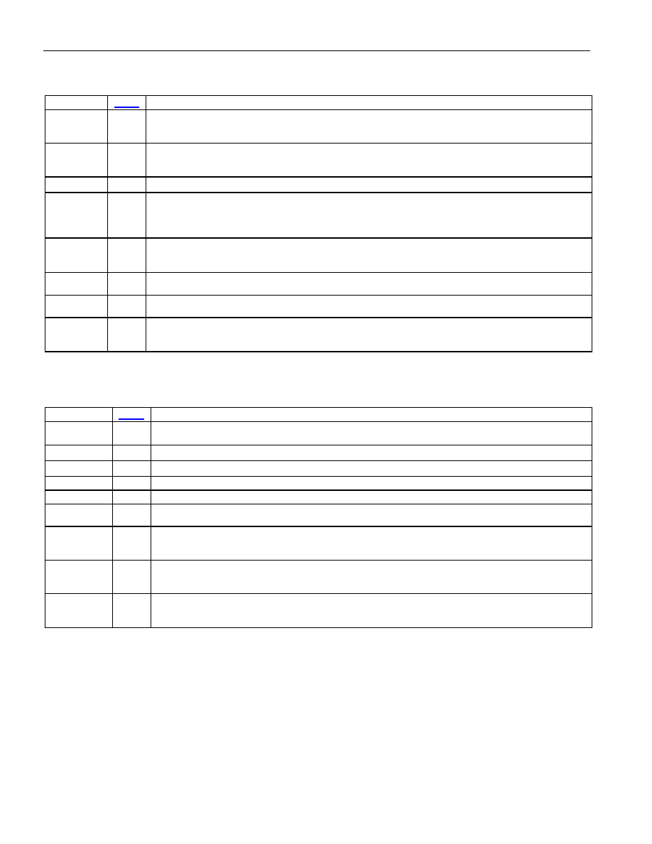
Table 6-E. Parallel Bus Mode Pin Descriptions
Note: These pins are active in parallel bus mode.
NAME
FUNCTION
MOT
I
Motorola-Style Parallel CPU Interface
0 = Parallel CPU interface is Intel-style
1 = Parallel CPU interface is Motorola-style
ALE
I
Address Latch Enable. This signal controls a latch on the A[3:0] inputs. For a nonmultiplexed parallel
CPU interface, ALE is wired high to make the latch transparent. For a multiplexed parallel CPU
interface, the falling edge of ALE latches the address.
CS
I
Chip Select (Active Low).
CS must be asserted to read or write internal registers.
WR / R/W
I
Write Enable (Active Low) or Read/Write Select. For the Intel-style parallel CPU interface (MOT =
0),
WR is asserted to write internal registers. For the Motorola-style parallel CPU interface (MOT = 1),
R/
W determines the type of bus transaction, with R/W = 1 indicating a read and R/W = 0 indicating a
write.
RD / DS
I
Read Enable (Active Low) or Data Strobe (Active Low). For the Intel-style parallel CPU interface
(MOT = 0),
RD is asserted to read internal registers. For the Motorola-style parallel CPU interface
(MOT = 1), the rising edge of
DS writes data to internal registers.
A[5:0]
I
Address Bus. These inputs specify the address of the internal register to be accessed. A5 is not
present on the DS3252. A5 and A4 are not present on the DS3251.
D[7:0]
I/O
Data Bus. These bidirectional lines are inputs during writes to internal registers and outputs during
reads.
INT
O
Interrupt Output (Active Low, Open Drain). This pin is forced low in response to one or more
unmasked, active interrupt sources within the device.
INT remains low until the interrupt is serviced or
masked.
Table 6-F. SPI Bus Mode Pin Descriptions
Note: These pins are active in SPI bus mode.
NAME
FUNCTION
MOT
,
RD, WR
I
Wire these pins low to enable SPI bus mode.
ALE
I
Wire this pin high when using SPI bus mode.
CS
I
Chip Select (Active Low).
CS must be asserted to read or write internal registers.
SCLK
I
Serial Clock for SPI Interface. SCLK is always driven by the SPI bus master.
SDI
I
Serial Data Input for SPI Interface. The SPI bus master transmits data to the device on this pin.
SDO
O
Serial Data Output for SPI Interface
The device transmits data to the SPI bus master on this pin.
CPHA
I
SPI Clock Phase
0 = data is latched on the leading edge of the SCLK pulse
1 = data is latched on the trailing edge of the SCLK pulse
CPOL
I
SPI Clock Polarity
0 = SCLK is normally low and pulses high during bus transactions
1 = SCLK is normally high and pulses low during bus transactions
INT
O
Interrupt Output (Active Low, Open Drain). This pin is forced low in response to one or more
unmasked, active interrupt sources within the device.
INT remains low until the interrupt is serviced or
masked.
Note 1:
PIN TYPES
I = input pin
IPU = input pin with internal 10k pullup
O = output pin
O3 = output pin that can be tri-stated
P = power-supply pin
相关PDF资料 |
PDF描述 |
|---|---|
| GCA32DRMH-S288 | CONN EDGECARD 64POS .125 EXTEND |
| EET-UQ2G471CA | CAP ALUM 470UF 400V 20% SNAP |
| UCY2G680MHD | CAP ALUM 68UF 400V 20% RADIAL |
| RCC22DCMS | CONN EDGECARD 44POS .100 WW |
| VE-JWK-EY-S | CONVERTER MOD DC/DC 40V 50W |
相关代理商/技术参数 |
参数描述 |
|---|---|
| DS3254N | 功能描述:网络控制器与处理器 IC Quad DS3/E3/STS-1 Line Interface Unit RoHS:否 制造商:Micrel 产品:Controller Area Network (CAN) 收发器数量: 数据速率: 电源电流(最大值):595 mA 最大工作温度:+ 85 C 安装风格:SMD/SMT 封装 / 箱体:PBGA-400 封装:Tray |
| DS3254N# | 功能描述:网络控制器与处理器 IC Quad DS3/E3/STS-1 Line Interface Unit RoHS:否 制造商:Micrel 产品:Controller Area Network (CAN) 收发器数量: 数据速率: 电源电流(最大值):595 mA 最大工作温度:+ 85 C 安装风格:SMD/SMT 封装 / 箱体:PBGA-400 封装:Tray |
| DS3254N+ | 功能描述:网络控制器与处理器 IC Quad DS3/E3/STS-1 Line Interface Unit RoHS:否 制造商:Micrel 产品:Controller Area Network (CAN) 收发器数量: 数据速率: 电源电流(最大值):595 mA 最大工作温度:+ 85 C 安装风格:SMD/SMT 封装 / 箱体:PBGA-400 封装:Tray |
| DS3254NA3 | 制造商:Maxim Integrated Products 功能描述:QUAD ENH DS3/E3 LIU REV A3 IND - Rail/Tube |
| DS3256 | 功能描述:网络控制器与处理器 IC X6 T3/E3 Line Interface Unit RoHS:否 制造商:Micrel 产品:Controller Area Network (CAN) 收发器数量: 数据速率: 电源电流(最大值):595 mA 最大工作温度:+ 85 C 安装风格:SMD/SMT 封装 / 箱体:PBGA-400 封装:Tray |
发布紧急采购,3分钟左右您将得到回复。