- 您现在的位置:买卖IC网 > PDF目录16258 > DS3254DK (Maxim Integrated Products)KIT DEMO FOR DS3254 PDF资料下载
参数资料
| 型号: | DS3254DK |
| 厂商: | Maxim Integrated Products |
| 文件页数: | 4/71页 |
| 文件大小: | 0K |
| 描述: | KIT DEMO FOR DS3254 |
| 产品培训模块: | Lead (SnPb) Finish for COTS Obsolescence Mitigation Program |
| 设计资源: | DS3254DK Gerber Files |
| 标准包装: | 1 |
| 主要目的: | 电信,线路接口单元(LIU) |
| 已用 IC / 零件: | DS3254 |
| 已供物品: | 板,CD |
第1页第2页第3页当前第4页第5页第6页第7页第8页第9页第10页第11页第12页第13页第14页第15页第16页第17页第18页第19页第20页第21页第22页第23页第24页第25页第26页第27页第28页第29页第30页第31页第32页第33页第34页第35页第36页第37页第38页第39页第40页第41页第42页第43页第44页第45页第46页第47页第48页第49页第50页第51页第52页第53页第54页第55页第56页第57页第58页第59页第60页第61页第62页第63页第64页第65页第66页第67页第68页第69页第70页第71页
DS3251/DS3252/DS3253/DS3254
12 of 71
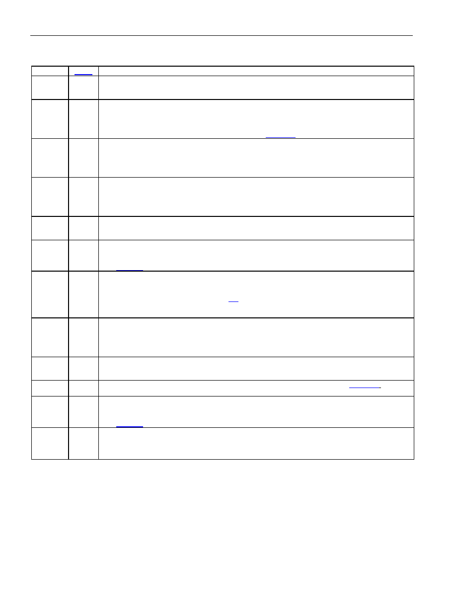
Table 6-D. Hardware Mode Pin Descriptions
Note: These pins are active in hardware mode.
NAME
FUNCTION
E3Mn
I
E3 Mode Enable
0 = DS3 operation
1 = E3 or STS-1 operation
STSn
I
STS-1 Mode Enable
When E3M = 1,
0 = E3 operation
1 = STS-1 operation
When E3M = 0, STS selects the DS3 AIS pattern. See Table 6-G.
LLBn,
RLBn
I
Local Loopback Select, Remote Loopback Select
{LLB, RLB} =
00 = no loopback
01 = remote loopback
10 = analog local loopback
11 = digital local loopback
RBIN
I
Receiver Binary Framer-Interface Enable
0 = Receiver framer interface is bipolar on the RPOS and RNEG pins. The B3ZS/HDB3 decoder is
disabled.
1 = Receiver framer interface is binary on the RDAT pin with the RLCV pin indicating line-code
violations. The B3ZS/HDB3 encoder is enabled.
RCINV
I
Receiver Clock Invert
0 = RPOS/RDAT and RNEG/RLCV update on the falling edge of RCLK.
1 = RPOS/RDAT and RNEG/RLCV update on the rising edge of RCLK.
RJAn
I
Receiver Jitter Attenuator Enable
0 = remove jitter attenuator from the receiver path
1 = insert jitter attenuator into the receiver path
See Table 6-I for more information.
RMONn
I
Receive Monitor-Preamp Enable. RMON determines whether or not the receiver’s preamp is enabled
to provide flat gain to the incoming signal before the AGC/equalizer block processes it. This feature
should be enabled when the device is being used to monitor signals that have been resistively
attenuated by a monitor jack. See Section 8.2 for more information.
0 = disable the monitor preamp
1 = enable the monitor preamp
TBIN
I
Transmitter Binary Framer-Interface Enable
0 = Transmitter framer interface is bipolar on the TPOS and TNEG pins. The B3ZS/HDB3 encoder is
disabled.
1 = Transmitter framer interface is binary on the TDAT pin. (TNEG is ignored and should be wired low.)
The B3ZS/HDB3 encoder is enabled.
TCINV
I
Transmitter Clock Invert
0 = TPOS/TDAT and TNEG are sampled on the rising edge of TCLK.
1 = TPOS/TDAT and TNEG are sampled on the falling edge of TCLK.
TDSAn,
TDSBn
I
Transmitter Data Select. These inputs select the source of the transmit data. See Table 6-G for
details.
TJAn
I
Transmitter Jitter Attenuator Enable
0 = remove jitter attenuator from the transmitter path
1 = insert jitter attenuator into the transmitter path
See Table 6-I for more information.
TLBOn
I
Transmitter Line Build-Out Enable. TLBO indicates cable length for waveform shaping in DS3 and
STS-1 modes. TLBO is ignored for E3 mode and should be wired high or low.
0 = cable length
≥ 225ft
1 = cable length < 225ft
相关PDF资料 |
PDF描述 |
|---|---|
| GCA32DRMH-S288 | CONN EDGECARD 64POS .125 EXTEND |
| EET-UQ2G471CA | CAP ALUM 470UF 400V 20% SNAP |
| UCY2G680MHD | CAP ALUM 68UF 400V 20% RADIAL |
| RCC22DCMS | CONN EDGECARD 44POS .100 WW |
| VE-JWK-EY-S | CONVERTER MOD DC/DC 40V 50W |
相关代理商/技术参数 |
参数描述 |
|---|---|
| DS3254N | 功能描述:网络控制器与处理器 IC Quad DS3/E3/STS-1 Line Interface Unit RoHS:否 制造商:Micrel 产品:Controller Area Network (CAN) 收发器数量: 数据速率: 电源电流(最大值):595 mA 最大工作温度:+ 85 C 安装风格:SMD/SMT 封装 / 箱体:PBGA-400 封装:Tray |
| DS3254N# | 功能描述:网络控制器与处理器 IC Quad DS3/E3/STS-1 Line Interface Unit RoHS:否 制造商:Micrel 产品:Controller Area Network (CAN) 收发器数量: 数据速率: 电源电流(最大值):595 mA 最大工作温度:+ 85 C 安装风格:SMD/SMT 封装 / 箱体:PBGA-400 封装:Tray |
| DS3254N+ | 功能描述:网络控制器与处理器 IC Quad DS3/E3/STS-1 Line Interface Unit RoHS:否 制造商:Micrel 产品:Controller Area Network (CAN) 收发器数量: 数据速率: 电源电流(最大值):595 mA 最大工作温度:+ 85 C 安装风格:SMD/SMT 封装 / 箱体:PBGA-400 封装:Tray |
| DS3254NA3 | 制造商:Maxim Integrated Products 功能描述:QUAD ENH DS3/E3 LIU REV A3 IND - Rail/Tube |
| DS3256 | 功能描述:网络控制器与处理器 IC X6 T3/E3 Line Interface Unit RoHS:否 制造商:Micrel 产品:Controller Area Network (CAN) 收发器数量: 数据速率: 电源电流(最大值):595 mA 最大工作温度:+ 85 C 安装风格:SMD/SMT 封装 / 箱体:PBGA-400 封装:Tray |
发布紧急采购,3分钟左右您将得到回复。