- 您现在的位置:买卖IC网 > PDF目录16594 > EVAL-AD7195EBZ (Analog Devices Inc)BOARD EVAL FOR AD7195 PDF资料下载
参数资料
| 型号: | EVAL-AD7195EBZ |
| 厂商: | Analog Devices Inc |
| 文件页数: | 20/45页 |
| 文件大小: | 0K |
| 描述: | BOARD EVAL FOR AD7195 |
| 设计资源: | EVAL-AD7195EBZ Schematic AD7195 Gerber Files |
| 标准包装: | 1 |
| 主要目的: | 接口,模拟前端(AFE) |
| 已用 IC / 零件: | AD7195 |
| 次要属性: | 图形用户界面,USB 接口 |
| 已供物品: | 板 |
第1页第2页第3页第4页第5页第6页第7页第8页第9页第10页第11页第12页第13页第14页第15页第16页第17页第18页第19页当前第20页第21页第22页第23页第24页第25页第26页第27页第28页第29页第30页第31页第32页第33页第34页第35页第36页第37页第38页第39页第40页第41页第42页第43页第44页第45页
AD7195
Rev. 0 | Page 26 of 44
ANALOG INPUT CHANNEL
The AD7195 has two differential/four pseudo differential
analog input channels, which can be buffered or unbuffered. In
buffered mode (the BUF bit in the configuration register is set
to 1), the input channel feeds into a high impedance input stage
of the buffer amplifier. Therefore, the input can tolerate signi-
ficant source impedances and is tailored for direct connection
to external resistive-type sensors such as strain gages or resis-
tance temperature detectors (RTDs).
When BUF = 0, the part operates in unbuffered mode. This
results in a higher analog input current. Note that this unbuffered
input path provides a dynamic load to the driving source.
Therefore, resistor/capacitor combinations on the input pins
can cause gain errors, depending on the output impedance of
the source that is driving the ADC input. Table 27 shows the
allowable external resistance/capacitance values for unbuffered
mode at a gain of 1 such that no gain error at the 20-bit level is
introduced.
Table 27. External R-C Combination for No 20-Bit Gain Error
C (pF)
R (Ω)
50
1.4 k
100
850
500
300
1000
230
5000
30
The absolute input voltage range in buffered mode is restricted
to a range between AGND + 250 mV and AVDD 250 mV. Care
must be taken in setting up the common-mode voltage so that
these limits are not exceeded. Otherwise, linearity and noise
performance degrades.
The absolute input voltage in unbuffered mode includes the
range between AGND 50 mV and AVDD + 50 mV. The
negative absolute input voltage limit does allow the possibility
of monitoring small true bipolar signals with respect to AGND.
PGA
When the gain stage is enabled, the output from the buffer
is applied to the input of the PGA. The presence of the PGA
means that signals of small amplitude can be gained within the
AD7195 while still maintaining excellent noise performance.
For example, when the gain is set to 128, the rms noise is 8.5 nV,
typically, when the output data rate is 4.7 Hz, which is equivalent
to 23 bits of effective resolution or 20.5 bits of noise-free resolution.
The AD7195 can be programmed to have a gain of 1, 8, 16, 32,
64, and 128 using Bit G2 to Bit G0 in the configuration register.
Therefore, with an external 2.5 V reference, the unipolar ranges
are from 0 mV to 19.53 mV to 0 V to 2.5 V and the bipolar
ranges are from ±19.53 mV to ±2.5 V.
The analog input range must be limited to ±(AVDD 1.25 V)/gain
because the PGA requires some headroom. Therefore, if AVDD =
5 V, the maximum analog input that can be applied to the
AD7195 is 0 to 3.75 V/gain in unipolar mode or ±3.75 V/gain
in bipolar mode.
REFERENCE
The ADC has a fully differential input capability for the refer-
ence channel. The common-mode range for these differential
inputs is from AGND to AVDD. The reference voltage REFIN
(REFIN(+) REFIN()) is AVDD nominal, but the AD7195
is functional with reference voltages from 1 V to AVDD. In
applications where the excitation (voltage or current) for the
transducer on the analog input also drives the reference voltage
for the part, the effect of the low frequency noise in the excita-
tion source is removed because the application is ratiometric. If
the AD7195 is used in a nonratiometric application, a low noise
reference should be used.
The reference input is unbuffered; therefore, excessive R-C
source impedances introduce gain errors. R-C values similar
to those in Table 27 are recommended for the reference inputs.
Deriving the reference input voltage across an external resistor
means that the reference input sees significant external source
impedance. External decoupling on the REFINx pins is not
recommended in this type of circuit configuration. Conversely,
if large decoupling capacitors are used on the reference inputs,
there should be no resistors in series with the reference inputs.
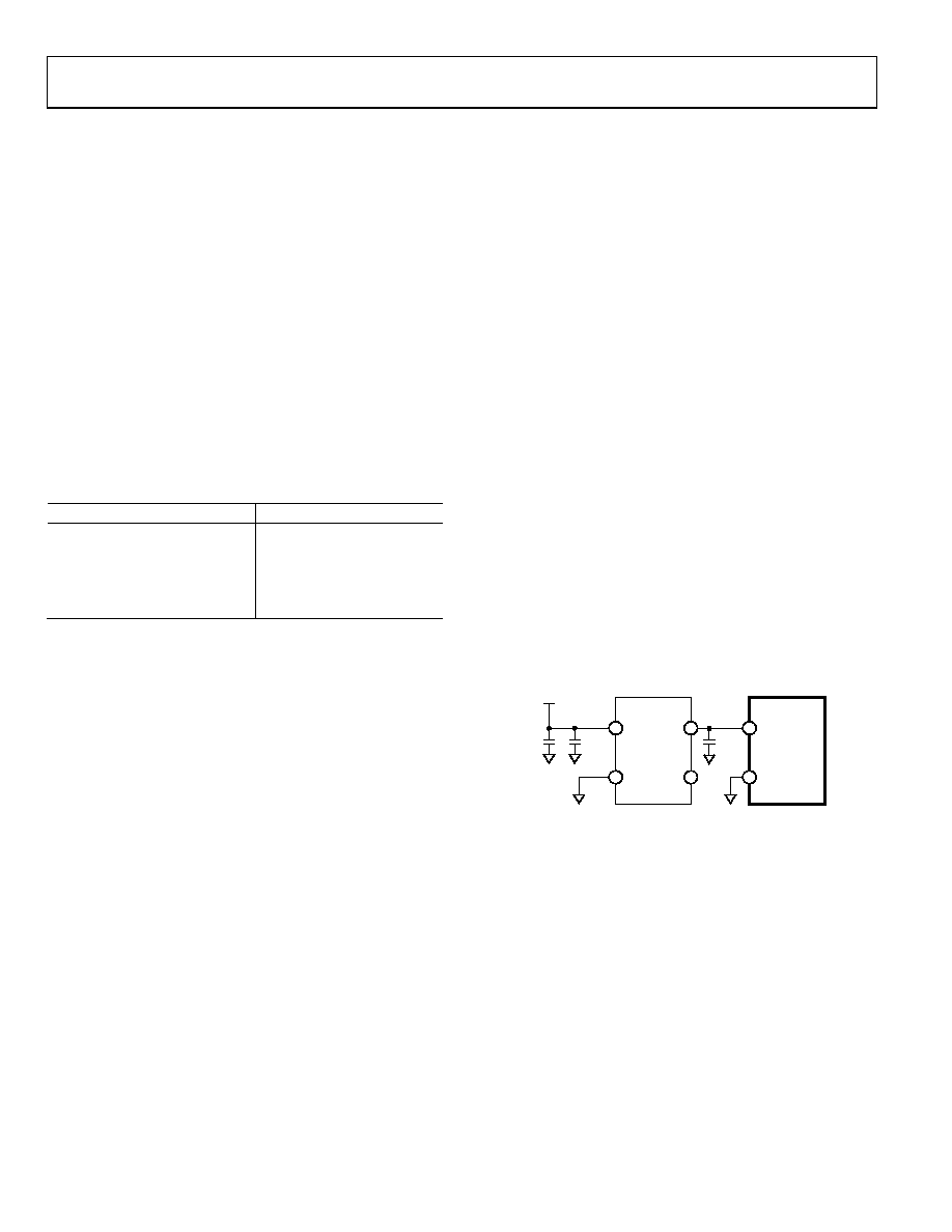
Recommended 2.5 V reference voltage sources for the AD7195
These references tolerate decoupling capacitors on REFIN(+)
without introducing gain errors in the system. Figure 19 shows the
recommended connections between the ADR421 and the AD7195.
4
2
0.1F
AVDD
ADR421
AD7195
VIN
GND
REFINx(+)
REFINx(–)
VOUT
TRIM
10F
4.7F
6
5
08
77
1-
03
7
Figure 19. ADR421 to AD7195 Connections
REFERENCE DETECT
The AD7195 includes on-chip circuitry to detect whether the
part has a valid reference for conversions or calibrations. This
feature is enabled when the REFDET bit in the configuration
register is set to 1. If the voltage between the REFIN(+) and
REFIN() pins is between 0.3 V and 0.6 V, the AD7195 detects
that it no longer has a valid reference. In this case, the NOREF
bit of the status register is set to 1. If the AD7195 is performing
normal conversions and the NOREF bit becomes active, the
conversion result is all 1s.
Therefore, it is not necessary to continuously monitor the status
of the NOREF bit when performing conversions. It is only
necessary to verify its status if the conversion result read from
the ADC data register is all 1s. If the AD7195 is performing
either an offset or full-scale calibration and the NOREF bit
becomes active, the updating of the respective calibration
相关PDF资料 |
PDF描述 |
|---|---|
| VI-B6B-EX | CONVERTER MOD DC/DC 95V 75W |
| ECM18DRPI | CONN EDGECARD 36POS DIP .156 SLD |
| EEM25DRMT | CONN EDGECARD 50POS .156 WW |
| V24C8C100BG3 | CONVERTER MOD DC/DC 8V 100W |
| H1WXH-2636G | IDC CABLE - HPL26H/AE26G/X |
相关代理商/技术参数 |
参数描述 |
|---|---|
| EVAL-AD7262EDZ | 功能描述:BOARD EVAL CONTROL AD7262 RoHS:是 类别:编程器,开发系统 >> 评估板 - 模数转换器 (ADC) 系列:- 产品培训模块:Obsolescence Mitigation Program 标准包装:1 系列:- ADC 的数量:1 位数:12 采样率(每秒):94.4k 数据接口:USB 输入范围:±VREF/2 在以下条件下的电源(标准):- 工作温度:-40°C ~ 85°C 已用 IC / 零件:MAX11645 已供物品:板,软件 |
| EVAL-AD7264EDZ | 功能描述:BOARD EVALUATION FOR AD7264 RoHS:是 类别:编程器,开发系统 >> 评估板 - 模数转换器 (ADC) 系列:- 产品培训模块:Obsolescence Mitigation Program 标准包装:1 系列:- ADC 的数量:1 位数:12 采样率(每秒):94.4k 数据接口:USB 输入范围:±VREF/2 在以下条件下的电源(标准):- 工作温度:-40°C ~ 85°C 已用 IC / 零件:MAX11645 已供物品:板,软件 |
| EVAL-AD7265CB | 制造商:AD 制造商全称:Analog Devices 功能描述:Differential/Single-Ended Input, Dual 1 MSPS, 12-Bit, 3-Channel SAR ADC |
| EVAL-AD7265CB1 | 制造商:AD 制造商全称:Analog Devices 功能描述:Differential Input, Dual 1 MSPS, 12-Bit, 3-Channel SAR ADC |
| EVAL-AD7265EDZ | 功能描述:BOARD EVAL FOR AD7265 A/D CONV RoHS:是 类别:编程器,开发系统 >> 评估板 - 模数转换器 (ADC) 系列:- 产品培训模块:Obsolescence Mitigation Program 标准包装:1 系列:- ADC 的数量:1 位数:12 采样率(每秒):94.4k 数据接口:USB 输入范围:±VREF/2 在以下条件下的电源(标准):- 工作温度:-40°C ~ 85°C 已用 IC / 零件:MAX11645 已供物品:板,软件 |
发布紧急采购,3分钟左右您将得到回复。