- 您现在的位置:买卖IC网 > PDF目录16594 > EVAL-AD7195EBZ (Analog Devices Inc)BOARD EVAL FOR AD7195 PDF资料下载
参数资料
| 型号: | EVAL-AD7195EBZ |
| 厂商: | Analog Devices Inc |
| 文件页数: | 28/45页 |
| 文件大小: | 0K |
| 描述: | BOARD EVAL FOR AD7195 |
| 设计资源: | EVAL-AD7195EBZ Schematic AD7195 Gerber Files |
| 标准包装: | 1 |
| 主要目的: | 接口,模拟前端(AFE) |
| 已用 IC / 零件: | AD7195 |
| 次要属性: | 图形用户界面,USB 接口 |
| 已供物品: | 板 |
第1页第2页第3页第4页第5页第6页第7页第8页第9页第10页第11页第12页第13页第14页第15页第16页第17页第18页第19页第20页第21页第22页第23页第24页第25页第26页第27页当前第28页第29页第30页第31页第32页第33页第34页第35页第36页第37页第38页第39页第40页第41页第42页第43页第44页第45页
AD7195
Rev. 0 | Page 33 of 44
BRIDGE POWER-DOWN SWITCH
In bridge applications, such as strain gauges and load cells, the
bridge itself consumes the majority of the current in the system.
For example, a 350 Ω load cell requires 15 mA of current when
excited with a 5 V supply. To minimize the current consumption
of the system, the bridge can be disconnected (when it is not
being used) using the bridge power-down switch. Figure 50
shows how the bridge power-down switch is used. The switch
can withstand 30 mA of continuous current, and it has an on
resistance of 10 Ω maximum.
CALIBRATION
The AD7195 provides four calibration modes that can be pro-
grammed via the mode bits in the mode register. These modes
are internal zero-scale calibration, internal full-scale calibration,
system zero-scale calibration, and system full-scale calibration.
A calibration can be performed at any time by setting the MD2
to MD0 bits in the mode register appropriately. A calibration
should be performed when the gain is changed. After each
conversion, the ADC conversion result is scaled using the ADC
calibration registers before being written to the data register.
The offset calibration coefficient is subtracted from the result
prior to multiplication by the full-scale coefficient.
To start a calibration, write the relevant value to the MD2 to
MD0 bits. The DOUT/RDY pin and the RDY bit in the status
register go high when the calibration is initiated. When the
calibration is complete, the contents of the corresponding
calibration registers are updated, the RDY bit in the status
register is reset, the DOUT/ RDY pin returns low (if CS is
low), and the AD7195 reverts to idle mode.
During an internal zero-scale or full-scale calibration, the res-
pective zero input and full-scale input are automatically connected
internally to the ADC input pins. A system calibration, however,
expects the system zero-scale and system full-scale voltages to
be applied to the ADC pins before initiating the calibration
mode. In this way, errors external to the ADC are removed.
From an operational point of view, treat a calibration like
another ADC conversion. A zero-scale calibration, if required,
must always be performed before a full-scale calibration. Set the
system software to monitor the RDY bit in the status register or
the DOUT/RDY pin to determine the end of calibration via a
polling sequence or an interrupt-driven routine.
With chop disabled, both an internal zero-scale calibration and a
system zero-scale calibration require a time equal to the settling
time, tSETTLE, (4/fADC for the sinc4 filter and 3/fADC for the sinc3 filter).
With chop enabled, an internal zero-scale calibration is not
needed because the ADC itself minimizes the offset continuously.
However, if an internal zero-scale calibration is performed, the
settling time, tSETTLE, (2/fADC) is required to perform the calibra-
tion. Similarly, a system zero-scale calibration requires a time of
tSETTLE to complete.
To perform an internal full-scale calibration, a full-scale input
voltage is automatically connected to the selected analog input
for this calibration. For a gain of 1, the time required for an
internal full-scale calibration is equal to tSETTLE. For higher gains,
the internal full-scale calibration requires a time of 2 × tSETTLE.
A full-scale calibration is recommended each time the gain of a
channel is changed to minimize the full-scale error.
A system full-scale calibration requires a time of tSETTLE. With
chop disabled, the zero-scale calibration (internal or system
zero-scale) should be performed before the system full-scale
calibration is initiated.
An internal zero-scale calibration, system zero-scale calibration
and system full-scale calibration can be performed at any output
data rate. An internal full-scale calibration can be performed at
any output data rate for which the filter word FS[9:0] is divisible
by 16, FS[9:0] being the decimal equivalent of the 10-bit word
written to Bit FS9 to Bit FS0 in the mode register. Therefore,
internal full-scale calibrations can be performed at output data
rates such as 10 Hz or 50 Hz when chop is disabled. Using these
lower output data rates results in better calibration accuracy.
The offset error is, typically, 100 μV/gain. If the gain is changed,
it is advisable to perform a calibration. A zero-scale calibration
(an internal zero-scale calibration or system zero-scale
calibration) reduces the offset error to the order of the noise.
The gain error of the AD7195 is factory calibrated at a gain of 1
with a 5 V power supply at ambient temperature. Following this
calibration, the gain error is 0.001%, typically, at 5 V. Table 28
shows the typical uncalibrated gain error for the different gain
settings. An internal full-scale calibration reduces the gain error
to 0.001%, typically, when the gain is equal to 1. For higher
gains, the gain error post internal full-scale calibration is
0.0075%, typically. A system full-sale calibration reduces the
gain error to the order of the noise.
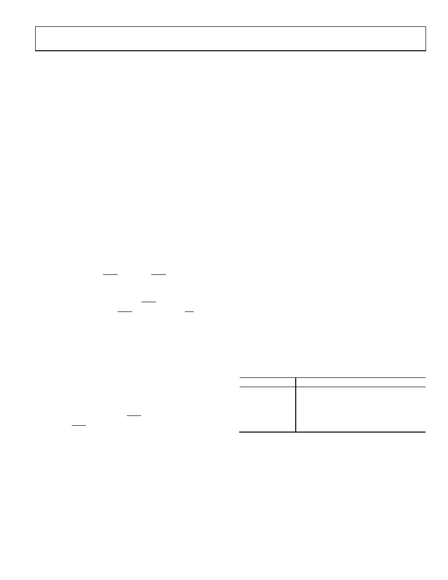
Table 28. Typical Precalibration Gain Error vs. Gain
Gain
Precalibration Gain Error (%)
8
0.11
16
0.20
32
0.23
64
0.29
128
0.39
The AD7195 gives the user access to the on-chip calibration
registers, allowing the microprocessor to read the calibration
coefficients of the device and also to write its own calibration
coefficients from prestored values in the EEPROM. A read of
the registers can be performed at any time. However, the ADC
must be placed in power-down or idle mode when writing to
the registers. The values in the calibration registers are 24-bits
wide. The span and offset of the part can also be manipulated
using the registers.
相关PDF资料 |
PDF描述 |
|---|---|
| VI-B6B-EX | CONVERTER MOD DC/DC 95V 75W |
| ECM18DRPI | CONN EDGECARD 36POS DIP .156 SLD |
| EEM25DRMT | CONN EDGECARD 50POS .156 WW |
| V24C8C100BG3 | CONVERTER MOD DC/DC 8V 100W |
| H1WXH-2636G | IDC CABLE - HPL26H/AE26G/X |
相关代理商/技术参数 |
参数描述 |
|---|---|
| EVAL-AD7262EDZ | 功能描述:BOARD EVAL CONTROL AD7262 RoHS:是 类别:编程器,开发系统 >> 评估板 - 模数转换器 (ADC) 系列:- 产品培训模块:Obsolescence Mitigation Program 标准包装:1 系列:- ADC 的数量:1 位数:12 采样率(每秒):94.4k 数据接口:USB 输入范围:±VREF/2 在以下条件下的电源(标准):- 工作温度:-40°C ~ 85°C 已用 IC / 零件:MAX11645 已供物品:板,软件 |
| EVAL-AD7264EDZ | 功能描述:BOARD EVALUATION FOR AD7264 RoHS:是 类别:编程器,开发系统 >> 评估板 - 模数转换器 (ADC) 系列:- 产品培训模块:Obsolescence Mitigation Program 标准包装:1 系列:- ADC 的数量:1 位数:12 采样率(每秒):94.4k 数据接口:USB 输入范围:±VREF/2 在以下条件下的电源(标准):- 工作温度:-40°C ~ 85°C 已用 IC / 零件:MAX11645 已供物品:板,软件 |
| EVAL-AD7265CB | 制造商:AD 制造商全称:Analog Devices 功能描述:Differential/Single-Ended Input, Dual 1 MSPS, 12-Bit, 3-Channel SAR ADC |
| EVAL-AD7265CB1 | 制造商:AD 制造商全称:Analog Devices 功能描述:Differential Input, Dual 1 MSPS, 12-Bit, 3-Channel SAR ADC |
| EVAL-AD7265EDZ | 功能描述:BOARD EVAL FOR AD7265 A/D CONV RoHS:是 类别:编程器,开发系统 >> 评估板 - 模数转换器 (ADC) 系列:- 产品培训模块:Obsolescence Mitigation Program 标准包装:1 系列:- ADC 的数量:1 位数:12 采样率(每秒):94.4k 数据接口:USB 输入范围:±VREF/2 在以下条件下的电源(标准):- 工作温度:-40°C ~ 85°C 已用 IC / 零件:MAX11645 已供物品:板,软件 |
发布紧急采购,3分钟左右您将得到回复。