- 您现在的位置:买卖IC网 > PDF目录16594 > EVAL-AD7195EBZ (Analog Devices Inc)BOARD EVAL FOR AD7195 PDF资料下载
参数资料
| 型号: | EVAL-AD7195EBZ |
| 厂商: | Analog Devices Inc |
| 文件页数: | 36/45页 |
| 文件大小: | 0K |
| 描述: | BOARD EVAL FOR AD7195 |
| 设计资源: | EVAL-AD7195EBZ Schematic AD7195 Gerber Files |
| 标准包装: | 1 |
| 主要目的: | 接口,模拟前端(AFE) |
| 已用 IC / 零件: | AD7195 |
| 次要属性: | 图形用户界面,USB 接口 |
| 已供物品: | 板 |
第1页第2页第3页第4页第5页第6页第7页第8页第9页第10页第11页第12页第13页第14页第15页第16页第17页第18页第19页第20页第21页第22页第23页第24页第25页第26页第27页第28页第29页第30页第31页第32页第33页第34页第35页当前第36页第37页第38页第39页第40页第41页第42页第43页第44页第45页
AD7195
Rev. 0 | Page 40 of 44
CHOP ENABLED (SINC3 FILTER)
With chop enabled, the ADC offset and offset drift are
minimized. The analog input pins are continuously swapped.
With the analog input pins connected in one direction, the
settling time of the sinc filter is allowed and a conversion is
recorded. The analog input pins invert and another settled
conversion is obtained. Subsequent conversions are averaged
to minimize the offset. This continuous swapping of the analog
input pins and the averaging of subsequent conversions means
that the offset drift is also minimized. With chop enabled, the
resolution increases by 0.5 bits. Using the sinc3 filter with chop
enabled is suitable for output data rates up to 320 Hz.
0
877
1-
0
36
SINC3/SINC4
MODULATOR
ADC
CHOP
Figure 45. Chop Enabled (Sinc3 Chop Enabled)
Output Data Rate and Settling Time (Sinc3 Chop
Enabled)
For the sinc3 filter, the output data rate is equal to
fADC = fCLK/(3 × 1024 × FS[9:0])
where:
fADC is the output data rate.
fCLK is the master clock (4.92 MHz nominal).
FS[9:0] is the decimal equivalent of Bit FS9 to Bit FS0 in the
mode register.
The value of FS[9:0] can be varied from 1 to 1023. This results
in an output data rate of 1.56 Hz to 1600 Hz. The settling time
is equal to
tSETTLE = 2/fADC
Table 34. Examples of Output Data Rates and the
Corresponding Settling Time (Chop Enabled, Sinc3 Filter)
FS[9:0]
Output Data Rate (Hz)
Settling Time (ms)
96
16.7
120
80
20
100
When a channel change occurs, the modulator and filter are
reset. The complete settling time is required to generate the first
conversion after the channel change. Subsequent conversions on
this channel occur at 1/fADC.
CHANNEL
CONVERSIONS
CHANNEL A
CH A
CH B
CHANNEL B
1/
fADC
CH B
0
87
71
-0
56
Figure 46. Channel Change (Sinc3 Chop Enable)
If conversions are performed on a single channel and a step
change occurs, the ADC does not detect the change in analog
input; therefore, it continues to output conversions at the
programmed output data rate. However, it is at least two
conversions later before the output data accurately reflects
the analog input. If the step change occurs while the ADC is
processing a conversion, then the ADC takes three conversions
after the step change to generate a fully settled result.
1/
fADC
ANALOG
INPUT
ADC
OUTPUT
FULLY
SETTLED
0
877
1-
0
57
Figure 47. Asynchronous Step Change in Analog Input (Sinc3 Chop Enabled)
The cutoff frequency f3dB is equal to
f3dB = 0.24 × fADC
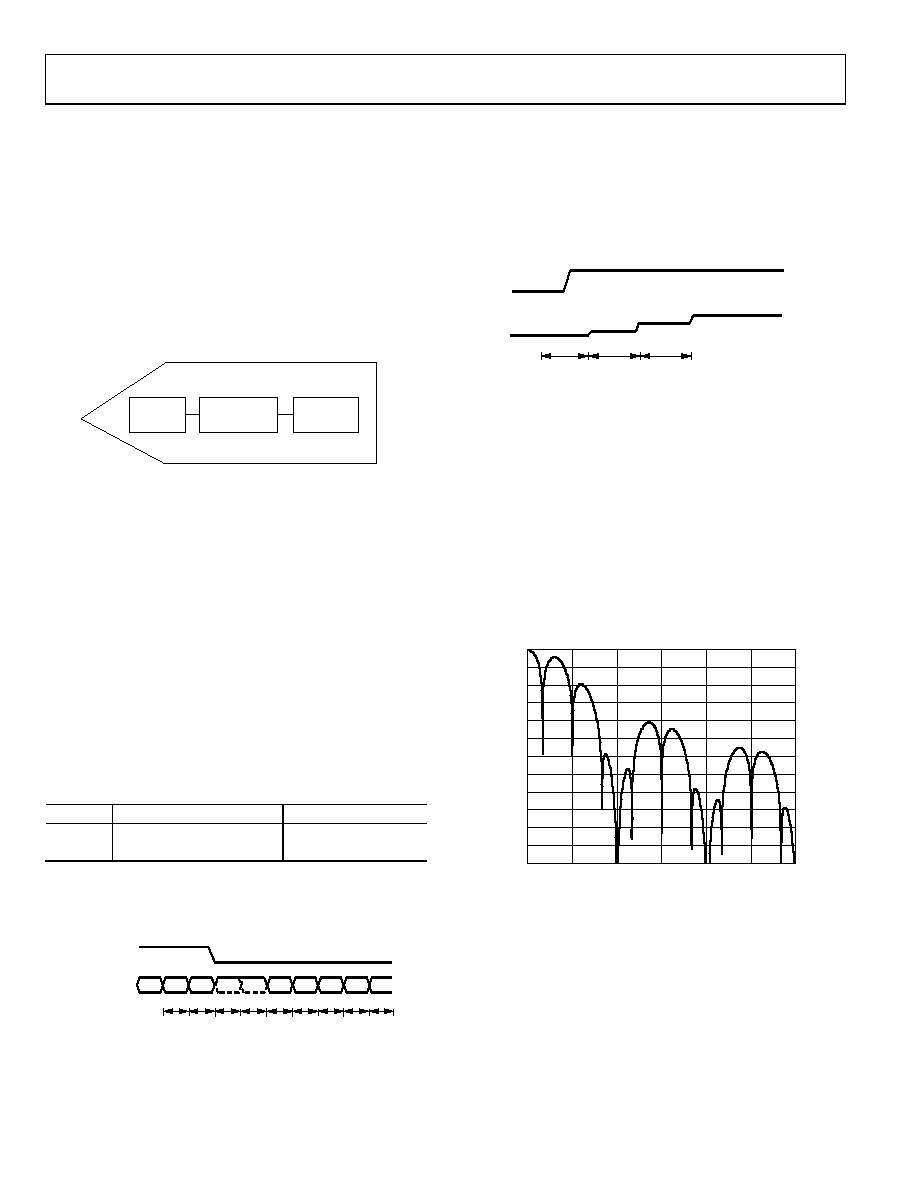
50 Hz/60 Hz Rejection (Sinc3 Chop Enabled)
When FS[9:0] is set to 96 and chopping is enabled, the filter
response shown in Figure 48 is obtained. The output data rate
is equal to 16.7 Hz for a 4.92 MHz master clock. The chopping
introduces notches at odd integer multiples of fADC/2. The
notches due to the sinc filter in addtion to the notches intro-
duced by the chopping means that simultaneous 50 Hz and
60 Hz rejection is achieved for an output data rate of 16.7 Hz.
The rejection at 50 Hz/60 Hz ± 1 Hz is typically 53 dB,
assuming a stable master clock.
–120
–110
–100
–90
–80
–70
–60
–50
–40
–30
–20
–10
0
25
50
75
100
125
150
FREQUENCY (Hz)
FIL
T
E
R
GA
IN
(
d
B
)
08
77
1-
0
58
Figure 48. Sinc3 Filter Response (FS[9:0] = 96, Chop Enabled)
相关PDF资料 |
PDF描述 |
|---|---|
| VI-B6B-EX | CONVERTER MOD DC/DC 95V 75W |
| ECM18DRPI | CONN EDGECARD 36POS DIP .156 SLD |
| EEM25DRMT | CONN EDGECARD 50POS .156 WW |
| V24C8C100BG3 | CONVERTER MOD DC/DC 8V 100W |
| H1WXH-2636G | IDC CABLE - HPL26H/AE26G/X |
相关代理商/技术参数 |
参数描述 |
|---|---|
| EVAL-AD7262EDZ | 功能描述:BOARD EVAL CONTROL AD7262 RoHS:是 类别:编程器,开发系统 >> 评估板 - 模数转换器 (ADC) 系列:- 产品培训模块:Obsolescence Mitigation Program 标准包装:1 系列:- ADC 的数量:1 位数:12 采样率(每秒):94.4k 数据接口:USB 输入范围:±VREF/2 在以下条件下的电源(标准):- 工作温度:-40°C ~ 85°C 已用 IC / 零件:MAX11645 已供物品:板,软件 |
| EVAL-AD7264EDZ | 功能描述:BOARD EVALUATION FOR AD7264 RoHS:是 类别:编程器,开发系统 >> 评估板 - 模数转换器 (ADC) 系列:- 产品培训模块:Obsolescence Mitigation Program 标准包装:1 系列:- ADC 的数量:1 位数:12 采样率(每秒):94.4k 数据接口:USB 输入范围:±VREF/2 在以下条件下的电源(标准):- 工作温度:-40°C ~ 85°C 已用 IC / 零件:MAX11645 已供物品:板,软件 |
| EVAL-AD7265CB | 制造商:AD 制造商全称:Analog Devices 功能描述:Differential/Single-Ended Input, Dual 1 MSPS, 12-Bit, 3-Channel SAR ADC |
| EVAL-AD7265CB1 | 制造商:AD 制造商全称:Analog Devices 功能描述:Differential Input, Dual 1 MSPS, 12-Bit, 3-Channel SAR ADC |
| EVAL-AD7265EDZ | 功能描述:BOARD EVAL FOR AD7265 A/D CONV RoHS:是 类别:编程器,开发系统 >> 评估板 - 模数转换器 (ADC) 系列:- 产品培训模块:Obsolescence Mitigation Program 标准包装:1 系列:- ADC 的数量:1 位数:12 采样率(每秒):94.4k 数据接口:USB 输入范围:±VREF/2 在以下条件下的电源(标准):- 工作温度:-40°C ~ 85°C 已用 IC / 零件:MAX11645 已供物品:板,软件 |
发布紧急采购,3分钟左右您将得到回复。