- 您现在的位置:买卖IC网 > PDF目录16594 > EVAL-AD7195EBZ (Analog Devices Inc)BOARD EVAL FOR AD7195 PDF资料下载
参数资料
| 型号: | EVAL-AD7195EBZ |
| 厂商: | Analog Devices Inc |
| 文件页数: | 33/45页 |
| 文件大小: | 0K |
| 描述: | BOARD EVAL FOR AD7195 |
| 设计资源: | EVAL-AD7195EBZ Schematic AD7195 Gerber Files |
| 标准包装: | 1 |
| 主要目的: | 接口,模拟前端(AFE) |
| 已用 IC / 零件: | AD7195 |
| 次要属性: | 图形用户界面,USB 接口 |
| 已供物品: | 板 |
第1页第2页第3页第4页第5页第6页第7页第8页第9页第10页第11页第12页第13页第14页第15页第16页第17页第18页第19页第20页第21页第22页第23页第24页第25页第26页第27页第28页第29页第30页第31页第32页当前第33页第34页第35页第36页第37页第38页第39页第40页第41页第42页第43页第44页第45页
AD7195
Rev. 0 | Page 38 of 44
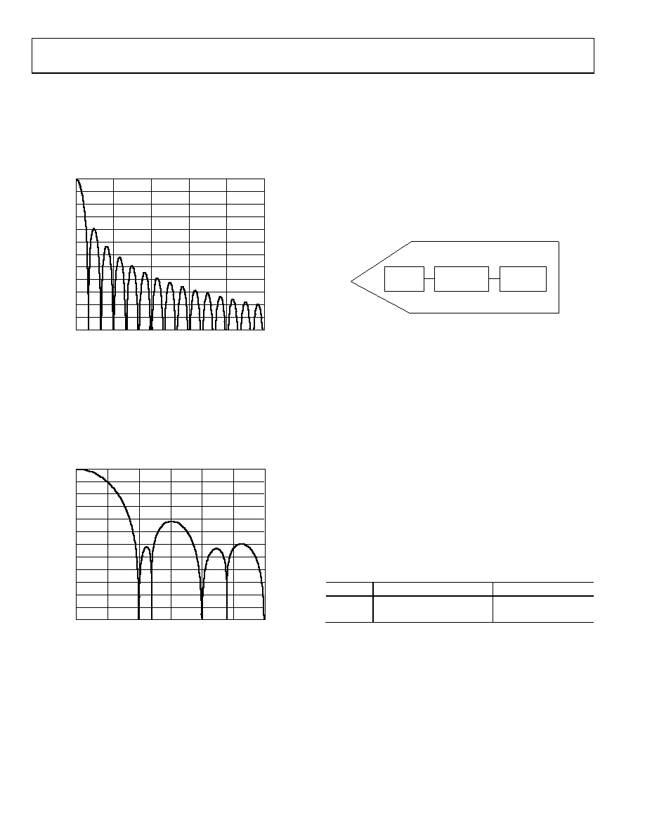
Simultaneous 50 Hz and 60 Hz rejection is obtained when
FS[9:0] is set to 480 (master clock = 4.92 MHz), as shown in
Figure 38. The output data rate is 10 Hz when zero latency is
disabled and 3.3 Hz when zero latency is enabled. The sinc3
filter has rejection of 100 dB minimum at 50 Hz ± 1 Hz and
60 Hz ± 1 Hz.
–120
–110
–100
–90
–80
–70
–60
–50
–40
–30
–20
–10
0
306090
120
150
FREQUENCY (Hz)
FI
L
T
E
R
GA
IN
(
d
B
)
08
77
1-
0
50
Figure 38. Sinc3 Filter Response (FS[9:0] = 480)
Simultaneous 50 Hz/60 Hz rejection is also achieved using the
REJ60 bit in the mode register. When FS[9:0] is programmed to
96 and the REJ60 bit is set to 1, notches are placed at both 50 Hz
and 60 Hz for a stable 4.92 MHz master clock. Figure 39 shows
the frequency response of the sinc3 filter with this configuration.
Assuming a stable clock, the rejection at 50 Hz/60 Hz (±1 Hz)
is in excess of 67 dB minimum.
–120
–110
–100
–90
–80
–70
–60
–50
–40
–30
–20
–10
0
25
50
75
100
125
150
FREQUENCY (Hz)
F
IL
T
E
R
GA
IN
(d
B
)
08
77
1-
05
1
Figure 39. Sinc3 Filter Response (FS[9:0] = 96, REJ60 = 1)
CHOP ENABLED (SINC4 FILTER)
With chop enabled, the ADC offset and offset drift are minimized.
The analog input pins are continuously swapped. With the
analog input pins connected in one direction, the settling time
of the sinc filter is allowed and a conversion is recorded. The
analog input pins are then inverted, and another settled conver-
sion is obtained. Subsequent conversions are averaged to
minimize the offset. This continuous swapping of the analog
input pins and the averaging of subsequent conversions means
that the offset drift is also minimized. With chop enabled, the
resolution increases by 0.5 bits.
0
877
1-
0
35
SINC3/SINC4
MODULATOR
ADC
CHOP
Figure 40. Chop Enabled
Output Data Rate and Settling Time (Sinc4 Chop
Enabled)
For the sinc4 filter, the output data rate is equal to
fADC = fCLK/(4 × 1024 × FS[9:0])
where:
fADC is the output data rate.
fCLK is the master clock (4.92 MHz nominal).
FS[9:0] is the decimal equivalent of Bit FS9 to Bit FS0 in the
mode register.
The value of FS[9:0] can be varied from 1 to 1023. This results
in an output data rate of 1.17 Hz to 1200 Hz. The settling time is
equal to
tSETTLE = 2/fADC
Table 33 gives some examples of FS[9:0] values and the corres-
ponding output data rates and settling times.
Table 33. Examples of Output Data Rates and the
Corresponding Settling Time
FS[9:0]
Output Data Rate (Hz)
Settling Time (ms)
96
12.5
160
80
15
133
相关PDF资料 |
PDF描述 |
|---|---|
| VI-B6B-EX | CONVERTER MOD DC/DC 95V 75W |
| ECM18DRPI | CONN EDGECARD 36POS DIP .156 SLD |
| EEM25DRMT | CONN EDGECARD 50POS .156 WW |
| V24C8C100BG3 | CONVERTER MOD DC/DC 8V 100W |
| H1WXH-2636G | IDC CABLE - HPL26H/AE26G/X |
相关代理商/技术参数 |
参数描述 |
|---|---|
| EVAL-AD7262EDZ | 功能描述:BOARD EVAL CONTROL AD7262 RoHS:是 类别:编程器,开发系统 >> 评估板 - 模数转换器 (ADC) 系列:- 产品培训模块:Obsolescence Mitigation Program 标准包装:1 系列:- ADC 的数量:1 位数:12 采样率(每秒):94.4k 数据接口:USB 输入范围:±VREF/2 在以下条件下的电源(标准):- 工作温度:-40°C ~ 85°C 已用 IC / 零件:MAX11645 已供物品:板,软件 |
| EVAL-AD7264EDZ | 功能描述:BOARD EVALUATION FOR AD7264 RoHS:是 类别:编程器,开发系统 >> 评估板 - 模数转换器 (ADC) 系列:- 产品培训模块:Obsolescence Mitigation Program 标准包装:1 系列:- ADC 的数量:1 位数:12 采样率(每秒):94.4k 数据接口:USB 输入范围:±VREF/2 在以下条件下的电源(标准):- 工作温度:-40°C ~ 85°C 已用 IC / 零件:MAX11645 已供物品:板,软件 |
| EVAL-AD7265CB | 制造商:AD 制造商全称:Analog Devices 功能描述:Differential/Single-Ended Input, Dual 1 MSPS, 12-Bit, 3-Channel SAR ADC |
| EVAL-AD7265CB1 | 制造商:AD 制造商全称:Analog Devices 功能描述:Differential Input, Dual 1 MSPS, 12-Bit, 3-Channel SAR ADC |
| EVAL-AD7265EDZ | 功能描述:BOARD EVAL FOR AD7265 A/D CONV RoHS:是 类别:编程器,开发系统 >> 评估板 - 模数转换器 (ADC) 系列:- 产品培训模块:Obsolescence Mitigation Program 标准包装:1 系列:- ADC 的数量:1 位数:12 采样率(每秒):94.4k 数据接口:USB 输入范围:±VREF/2 在以下条件下的电源(标准):- 工作温度:-40°C ~ 85°C 已用 IC / 零件:MAX11645 已供物品:板,软件 |
发布紧急采购,3分钟左右您将得到回复。