- 您现在的位置:买卖IC网 > PDF目录67593 > FX980L6 (CML MICROSYSTEMS PLC) SPECIALTY CONSUMER CIRCUIT, PQCC44 PDF资料下载
参数资料
| 型号: | FX980L6 |
| 厂商: | CML MICROSYSTEMS PLC |
| 元件分类: | 消费家电 |
| 英文描述: | SPECIALTY CONSUMER CIRCUIT, PQCC44 |
| 封装: | PLASTIC, LCC-44 |
| 文件页数: | 64/86页 |
| 文件大小: | 821K |
| 代理商: | FX980L6 |
第1页第2页第3页第4页第5页第6页第7页第8页第9页第10页第11页第12页第13页第14页第15页第16页第17页第18页第19页第20页第21页第22页第23页第24页第25页第26页第27页第28页第29页第30页第31页第32页第33页第34页第35页第36页第37页第38页第39页第40页第41页第42页第43页第44页第45页第46页第47页第48页第49页第50页第51页第52页第53页第54页第55页第56页第57页第58页第59页第60页第61页第62页第63页当前第64页第65页第66页第67页第68页第69页第70页第71页第72页第73页第74页第75页第76页第77页第78页第79页第80页第81页第82页第83页第84页第85页第86页
TETRA Baseband Processor
FX980
1997 Consumer Microcircuits Limited
67
D/980/3
RxDataAccess
Title:
Rx Data path Access point.
Address:
$0x38 to $0x3B (mapped over 4 locations)
Function:
RW
Description:
This register block allows direct access to the Rx Data path values just after the 59-tap (Rx anti-
alias) filter. Both read and write operations are permitted. A read operation reads the signal
values on the I and Q channels. A write operation will write data to the Rx Data path operator
output. To prevent normal Rx data overwriting this value the RxDPAccessSel bit in the
LoopBackCtrl register should be set active. The MSB read data register is buffered to enable
access of a discrete sample value (if this register was not buffered, data from different sample
periods could be in the MSB and LSB registers). Therefore the LSB register must be read first
for correct operation.
Bit
Name
Active State
Function
Address $0x38
7:0
RxDPIDataLSB
Data RW
Least significant 8 bits of the RxDPIData register. This
register must be read before its associated MSB register.
Address $0x39
7:0
RxDPIDataMSB
Data RW
Most significant 8 bits of the RxDPIData register.
Address $0x3A
7:0
RxDPQDataLSB
Data RW
Least significant 8 bits of the RxDPQData register. This
register must be read before its associated MSB register.
Address $0x3B
7:0
RxDPQDataMSB
Data RW
Most significant 8 bits of the RxDPQData register.
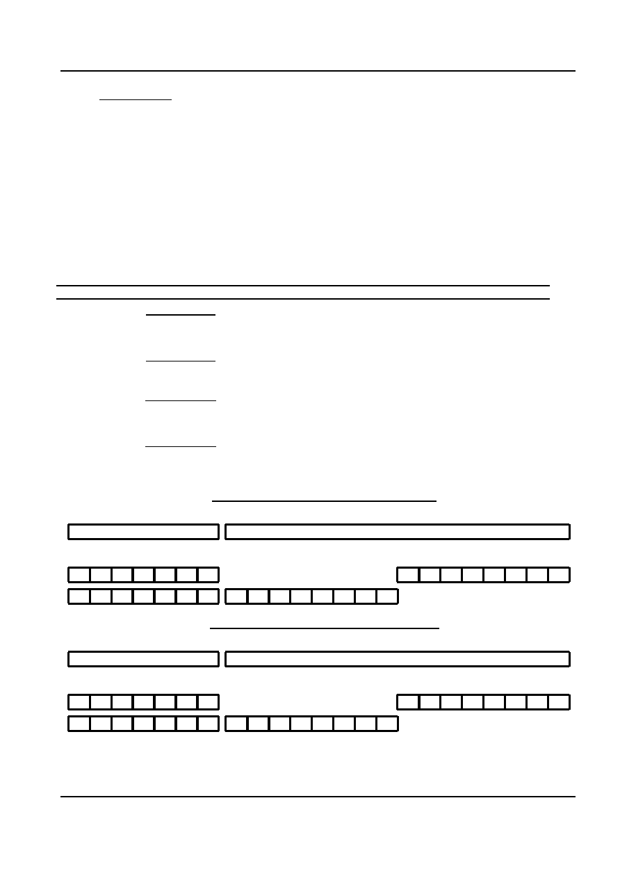
Address and Data format for RxDPIData access
D1 D0
D7 D6 D5 D4 D3 D2
D15 D14 D13 D12 D11 D10 D9 D8
0
Data field [15:0]
1
Address field
[6:0]
0
1
0
1
0
1
0
1
Address and Data format for RxDPQData access
D1 D0
D7 D6 D5 D4 D3 D2
D15 D14 D13 D12 D11 D10 D9 D8
0
Data field [15:0]
1
Address field
[6:0]
0
1
0
1
0
1
0
1
相关PDF资料 |
PDF描述 |
|---|---|
| FXO-HC320-0.7500M | CRYSTAL OSCILLATOR, CLOCK, 0.75 MHz, HCMOS OUTPUT |
| FXO-HC320-180.00M | CRYSTAL OSCILLATOR, CLOCK, 180 MHz, HCMOS OUTPUT |
| FXO-HC325-180.00M | CRYSTAL OSCILLATOR, CLOCK, 180 MHz, HCMOS OUTPUT |
| FXO-HC325R-106.25M | CRYSTAL OSCILLATOR, CLOCK, 106.25 MHz, HCMOS OUTPUT |
| FXO-HC320R-106.25M | CRYSTAL OSCILLATOR, CLOCK, 106.25 MHz, HCMOS OUTPUT |
相关代理商/技术参数 |
参数描述 |
|---|---|
| FX981006 | 制造商:Thomas & Betts 功能描述: |
| FX-991ES | 制造商:CASIO 功能描述:CALCULATOR |
| FX-991ES+ | 制造商:CASIO 功能描述:CALCULATOR ((NS)) |
| FX992S | 制造商:CASIO 功能描述:CALCULATOR SCIENTIFIC 制造商:CASIO 功能描述:CALCULATOR, SCIENTIFIC |
| FX996 | 制造商:BACO Controls Inc 功能描述: |
发布紧急采购,3分钟左右您将得到回复。