- 您现在的位置:买卖IC网 > PDF目录223993 > HY5DU56422ALF-J (HYNIX SEMICONDUCTOR INC) 64M X 4 DDR DRAM, 0.7 ns, PBGA60 PDF资料下载
参数资料
| 型号: | HY5DU56422ALF-J |
| 厂商: | HYNIX SEMICONDUCTOR INC |
| 元件分类: | DRAM |
| 英文描述: | 64M X 4 DDR DRAM, 0.7 ns, PBGA60 |
| 封装: | FBGA-60 |
| 文件页数: | 32/36页 |
| 文件大小: | 395K |
| 代理商: | HY5DU56422ALF-J |
第1页第2页第3页第4页第5页第6页第7页第8页第9页第10页第11页第12页第13页第14页第15页第16页第17页第18页第19页第20页第21页第22页第23页第24页第25页第26页第27页第28页第29页第30页第31页当前第32页第33页第34页第35页第36页
Rev. 0.1/Apr. 02
5
HY5DU56422A(L)F
HY5DU56822A(L)F
HY5DU561622A(L)F
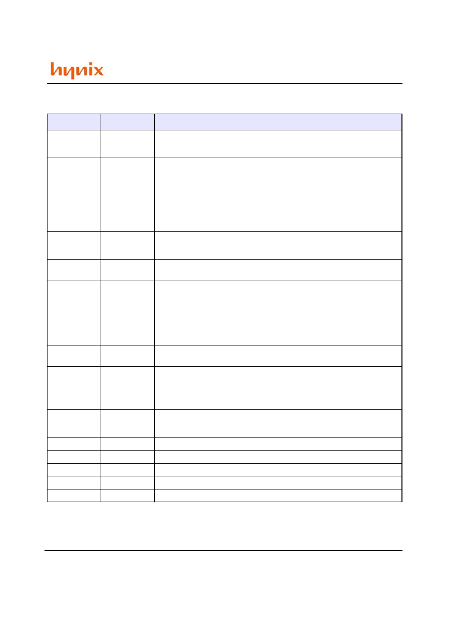
PIN DESCRIPTION
PIN
TYPE
DESCRIPTION
CK, /CK
Input
Clock: CK and /CK are differential clock inputs. All address and control input signals are
sampled on the crossing of the positive edge of CK and negative edge of /CK. Output
(read) data is referenced to the crossings of CK and /CK (both directions of crossing).
CKE
Input
Clock Enable: CKE HIGH activates, and CKE LOW deactivates internal clock signals, and
device input buffers and output drivers. Taking CKE LOW provides PRECHARGE POWER
DOWN and SELF REFRESH operation (all banks idle), or ACTIVE POWER DOWN (row
ACTIVE in any bank). CKE is synchronous for POWER DOWN entry and exit, and for SELF
REFRESH entry. CKE is asynchronous for SELF REFRESH exit, and for output disable. CKE
must be maintained high throughout READ and WRITE accesses. Input buffers, excluding
CK, /CK and CKE are disabled during POWER DOWN. Input buffers, excluding CKE are
disabled during SELF REFRESH. CKE is an SSTL_2 input, but will detect an LVCMOS LOW
level after Vdd is applied.
/CS
Input
Chip Select : Enables or disables all inputs except CK, /CK, CKE, DQS and DM. All com-
mands are masked when CS is registered high. CS provides for external bank selection on
systems with multiple banks. CS is considered part of the command code.
BA0, BA1
Input
Bank Address Inputs: BA0 and BA1 define to which bank an ACTIVE, Read, Write or PRE-
CHARGE command is being applied.
A0 ~ A12
Input
Address Inputs: Provide the row address for ACTIVE commands, and the column address
and AUTO PRECHARGE bit for READ/WRITE commands, to select one location out of the
memory array in the respective bank. A10 is sampled during a precharge command to
determine whether the PRECHARGE applies to one bank (A10 LOW) or all banks (A10
HIGH). If only one bank is to be precharged, the bank is selected by BA0, BA1. The
address inputs also provide the op code during a MODE REGISTER SET command. BA0
and BA1 define which mode register is loaded during the MODE REGISTER SET command
(MRS or EMRS).
/RAS, /CAS, /WE
Input
Command Inputs: /RAS, /CAS and /WE (along with /CS) define the command being
entered.
DM
(LDM, UDM)
Input
Input Data Mask: DM is an input mask signal for write data. Input data is masked when
DM is sampled HIGH along with that input data during a WRITE access. DM is sampled
on both edges of DQS. Although DM pins are input only, the DM loading matches the DQ
and DQS loading. For the x16, LDM corresponds to the data on DQ0-Q7; UDM corre-
sponds to the data on DQ8-Q15.
DQS
(LDQS, UDQS)
I/O
Data Strobe: Output with read data, input with write data. Edge aligned with read data,
centered in write data. Used to capture write data. For the x16, LDQS corresponds to the
data on DQ0-Q7; UDQS corresponds to the data on DQ8-Q15.
DQ
I/O
Data input / output pin : Data bus
VDD/VSS
Supply
Power supply for internal circuits and input buffers.
VDDQ/VSSQ
Supply
Power supply for output buffers for noise immunity.
VREF
Supply
Reference voltage for inputs for SSTL interface.
NC
No connection.
相关PDF资料 |
PDF描述 |
|---|---|
| HY5MS5B6LF-H | 16M X 16 DDR DRAM, 6.5 ns, PBGA60 |
| HY5PS1G831ALFP-C4 | 128M X 8 DDR DRAM, PBGA68 |
| HY5PS1G831ALFP-Y5 | 128M X 8 DDR DRAM, PBGA68 |
| HY5RS573225AFP-16L | 8M X 32 DDR DRAM, 0.28 ns, PBGA136 |
| HY5V28CF-S | 16M X 8 SYNCHRONOUS DRAM, 6 ns, PBGA54 |
相关代理商/技术参数 |
参数描述 |
|---|---|
| HY5DU56422ALT | 制造商:未知厂家 制造商全称:未知厂家 功能描述:64Mx4|2.5V|8K|J/M/K/H/L|DDR SDRAM - 256M |
| HY5DU56422ALT-H | 制造商:HYNIX 制造商全称:Hynix Semiconductor 功能描述:256M-S DDR SDRAM |
| HY5DU56422ALT-J | 制造商:HYNIX 制造商全称:Hynix Semiconductor 功能描述:256M-S DDR SDRAM |
| HY5DU56422ALT-K | 制造商:HYNIX 制造商全称:Hynix Semiconductor 功能描述:256M-S DDR SDRAM |
| HY5DU56422ALT-L | 制造商:HYNIX 制造商全称:Hynix Semiconductor 功能描述:256M-S DDR SDRAM |
发布紧急采购,3分钟左右您将得到回复。