- 您现在的位置:买卖IC网 > PDF目录4588 > IDT72V51246L6BB8 (IDT, Integrated Device Technology Inc)IC FLOW CTRL MULTI QUEUE 256-BGA PDF资料下载
参数资料
| 型号: | IDT72V51246L6BB8 |
| 厂商: | IDT, Integrated Device Technology Inc |
| 文件页数: | 3/56页 |
| 文件大小: | 0K |
| 描述: | IC FLOW CTRL MULTI QUEUE 256-BGA |
| 标准包装: | 1,000 |
| 类型: | 多队列流量控制 |
| 安装类型: | 表面贴装 |
| 封装/外壳: | 256-BBGA |
| 供应商设备封装: | 256-BGA(17x17) |
| 包装: | 带卷 (TR) |
| 其它名称: | 72V51246L6BB8 |
第1页第2页当前第3页第4页第5页第6页第7页第8页第9页第10页第11页第12页第13页第14页第15页第16页第17页第18页第19页第20页第21页第22页第23页第24页第25页第26页第27页第28页第29页第30页第31页第32页第33页第34页第35页第36页第37页第38页第39页第40页第41页第42页第43页第44页第45页第46页第47页第48页第49页第50页第51页第52页第53页第54页第55页第56页
11
COMMERCIALANDINDUSTRIAL
TEMPERATURERANGES
IDT72V51236/72V51246/72V51256 3.3V, MULTI-QUEUE FLOW-CONTROL DEVICES
(4 QUEUES) 36 BIT WIDE CONFIGURATION 589,824, 1,179,648 and 2,359,296 bits
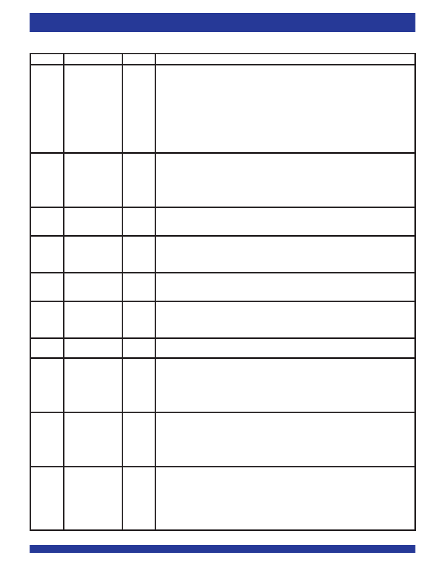
PIN DESCRIPTIONS (CONTINUED)
Symbol
Name
I/O TYPE
Description
SENO
Serial Output Enable
LVTTL
This output is used to indicate that serial programming or default programming of the multi-queue device
OUTPUT
has been completed.
SENOfollowsSENIonceprogrammingofadeviceiscomplete.Therefore,SENO
will go LOW after programming provided
SENI is LOW, onceSENI istakenHIGHagain,SENOwillalso
go HIGH. When the
SENOoutputgoesLOW,thedeviceisreadytobeginnormalread/writeoperations.
If multiple devices are cascaded and serial programming of the devices will be used, the
SENO output
should be connected to the
SENI input of the next device in the chain. When serial programming of the
first device is complete,
SENO will go LOW, thereby taking the SENI input of the next device LOW and
so on throughout the chain. When a given device in the chain is fully programmed the
SENO output
essentiallyfollowsthe
SENIinput.TheusershouldmonitortheSENOoutputofthefinaldeviceinthechain.
When this output goes LOW, serial loading of all devices has been completed.
SI
Serial In
LVTTL
During serial programming this pin is loaded with the serial data that will configure the multi-queue
INPUT
devices. Data present on SI will be loaded on a rising edge of SCLK provided that
SENI is LOW. In
expansion mode the serial data input is loaded into the first device in a chain. When that device is loaded
and its
SENO has gone LOW, the data present on SI will be directly output to the SO output. The SO pin
of the first device connects to the SI pin of the second and so on. The multi-queue device setup registers
are shift registers.
SO
Serial Out
LVTTL
This output is used in expansion mode and allows serial data to be passed through devices in the chain
OUTPUT
to complete programming of all devices. The SI of a device connects to SO of the previous device in the
chain. The SO of the final device in a chain should not be connected.
TCK(2)
JTAG Clock
LVTTL
Clock input for JTAG function. One of four terminals required by IEEE Standard 1149.1-1990. Test
INPUT
operations of the device are synchronous to TCK. Data from TMS and TDI are sampled on the rising edge
of TCK and outputs change on the falling edge of TCK. If the JTAG function is not used this signal needs
to be tied to GND.
TDI(2)
JTAG Test Data
LVTTL
One of four terminals required by IEEE Standard 1149.1-1990. During the JTAG boundary scan
Input
INPUT
operation,test data serially loaded via the TDI on the rising edge of TCK to either the Instruction Register,
ID Register and Bypass Register. An internal pull-up resistor forces TDI HIGH if left unconnected.
TDO(2)
JTAG Test Data
LVTTL
One of four terminals required by IEEE Standard 1149.1-1990. During the JTAG boundary scan
Output
OUTPUT
operation,testdataseriallyloadedoutputviatheTDOonthefallingedgeofTCKfromeithertheInstruction
Register, ID Register and Bypass Register. This output is high impedance except when shifting, while in
SHIFT-DR and SHIFT-IR controller states.
TMS(2)
JTAG Mode Select
LVTTL
TMS is a serial input pin. One of four terminals required by IEEE Standard 1149.1-1990. TMS directs the
INPUT
device through its TAP controller states. An internal pull-up resistor forces TMS HIGH if left unconnected.
TRST(2)
JTAG Reset
LVTTL
TRSTisanasynchronousresetpinfortheJTAGcontroller.TheJTAGTAPcontrollerdoesnotautomatically
INPUT
resetuponpower-up,thusitmustberesetbyeitherthissignalorbysettingTMS=HIGHforfiveTCKcycles.
If the TAP controller is not properly reset then the outputs will always be in high-impedance. If the JTAG
function is used but the user does not want to use
TRST, then TRST can be tied with MRS to ensure
proper queue operation. If the JTAG function is not used then this signal needs to be tied to GND. An
internal pull-up resistor forces
TRST HIGH if left unconnected.
WADEN
Write Address Enable
LVTTL
The WADEN input is used in conjunction with WCLK and the WRADD address bus to select a queue to
INPUT
be written in to. A queue addressed via the WRADD bus is selected on the rising edge of WCLK provided
thatWADENisHIGH.WADENshouldbeasserted(HIGH)onlyduringaqueuechangecycle(s).WADEN
shouldnotbepermanentlytiedHIGH.WADENcannotbeHIGHforthesameWCLKcycleasFSTR.Note,
that a write queue selection cannot be made, (WADEN must NOT go active) until programming of the
part has been completed and
SENO has gone LOW.
WCLK
WriteClock
LVTTL
When enabled by
WEN, the rising edge of WCLK writes data into the selected queue via the input bus,
INPUT
Din. The queue to be written to is selected via the WRADD address bus and a rising edge of WCLK while
WADENisHIGH.ArisingedgeofWCLKinconjunctionwithFSTRandWRADDwillalsoselectthedevice
to be placed on the
PAFn bus during direct flag operation. During polled flag operation the PAFn bus is
cycled with respect to WCLK and the FSYNC signal is synchronized to WCLK. The
PAFn, PAF and FF
outputs are all synchronized to WCLK. During device expansion the FXO and FXI signals are based on
WCLK. The WCLK must be continuous and free-running.
相关PDF资料 |
PDF描述 |
|---|---|
| LFXP6E-4Q208I | IC FPGA 5.8KLUTS 142I/O 208-PQFP |
| LFXP6C-5Q208C | IC FPGA 5.8KLUTS 142I/O 208-PQFP |
| LFXP6C-4Q208I | IC FPGA 5.8KLUTS 142I/O 208-PQFP |
| LFXP6E-4QN208I | IC FPGA 5.8KLUTS 208PQFP |
| LFXP6E-5QN208C | IC FPGA 5.8KLUTS 208PQFP |
相关代理商/技术参数 |
参数描述 |
|---|---|
| IDT72V51246L7-5BB | 功能描述:IC FLOW CTRL MULTI QUEUE 256-BGA RoHS:否 类别:集成电路 (IC) >> 专用 IC 系列:- 产品培训模块:Lead (SnPb) Finish for COTS Obsolescence Mitigation Program 标准包装:1 系列:- 类型:调帧器 应用:数据传输 安装类型:表面贴装 封装/外壳:400-BBGA 供应商设备封装:400-PBGA(27x27) 包装:散装 |
| IDT72V51246L7-5BB8 | 功能描述:IC FLOW CTRL MULTI QUEUE 256-BGA RoHS:否 类别:集成电路 (IC) >> 专用 IC 系列:- 产品培训模块:Lead (SnPb) Finish for COTS Obsolescence Mitigation Program 标准包装:1 系列:- 类型:调帧器 应用:数据传输 安装类型:表面贴装 封装/外壳:400-BBGA 供应商设备封装:400-PBGA(27x27) 包装:散装 |
| IDT72V51246L7-5BBI | 功能描述:IC FLOW CTRL MULTI QUEUE 256-BGA RoHS:否 类别:集成电路 (IC) >> 专用 IC 系列:- 产品培训模块:Lead (SnPb) Finish for COTS Obsolescence Mitigation Program 标准包装:1 系列:- 类型:调帧器 应用:数据传输 安装类型:表面贴装 封装/外壳:400-BBGA 供应商设备封装:400-PBGA(27x27) 包装:散装 |
| IDT72V51253L6BB | 功能描述:IC FLOW CTRL MULTI QUEUE 256-BGA RoHS:否 类别:集成电路 (IC) >> 专用 IC 系列:- 产品培训模块:Lead (SnPb) Finish for COTS Obsolescence Mitigation Program 标准包装:1 系列:- 类型:调帧器 应用:数据传输 安装类型:表面贴装 封装/外壳:400-BBGA 供应商设备封装:400-PBGA(27x27) 包装:散装 |
| IDT72V51253L6BB8 | 功能描述:IC FLOW CTRL MULTI QUEUE 256-BGA RoHS:否 类别:集成电路 (IC) >> 专用 IC 系列:- 产品培训模块:Lead (SnPb) Finish for COTS Obsolescence Mitigation Program 标准包装:1 系列:- 类型:调帧器 应用:数据传输 安装类型:表面贴装 封装/外壳:400-BBGA 供应商设备封装:400-PBGA(27x27) 包装:散装 |
发布紧急采购,3分钟左右您将得到回复。