- 您现在的位置:买卖IC网 > PDF目录4588 > IDT72V51246L6BB8 (IDT, Integrated Device Technology Inc)IC FLOW CTRL MULTI QUEUE 256-BGA PDF资料下载
参数资料
| 型号: | IDT72V51246L6BB8 |
| 厂商: | IDT, Integrated Device Technology Inc |
| 文件页数: | 55/56页 |
| 文件大小: | 0K |
| 描述: | IC FLOW CTRL MULTI QUEUE 256-BGA |
| 标准包装: | 1,000 |
| 类型: | 多队列流量控制 |
| 安装类型: | 表面贴装 |
| 封装/外壳: | 256-BBGA |
| 供应商设备封装: | 256-BGA(17x17) |
| 包装: | 带卷 (TR) |
| 其它名称: | 72V51246L6BB8 |
第1页第2页第3页第4页第5页第6页第7页第8页第9页第10页第11页第12页第13页第14页第15页第16页第17页第18页第19页第20页第21页第22页第23页第24页第25页第26页第27页第28页第29页第30页第31页第32页第33页第34页第35页第36页第37页第38页第39页第40页第41页第42页第43页第44页第45页第46页第47页第48页第49页第50页第51页第52页第53页第54页当前第55页第56页
8
IDT72V51236/72V51246/72V51256 3.3V, MULTI-QUEUE FLOW-CONTROL DEVICES
(4 QUEUES) 36 BIT WIDE CONFIGURATION 589,824, 1,179,648 and 2,359,296 bits
COMMERCIALANDINDUSTRIAL
TEMPERATURERANGES
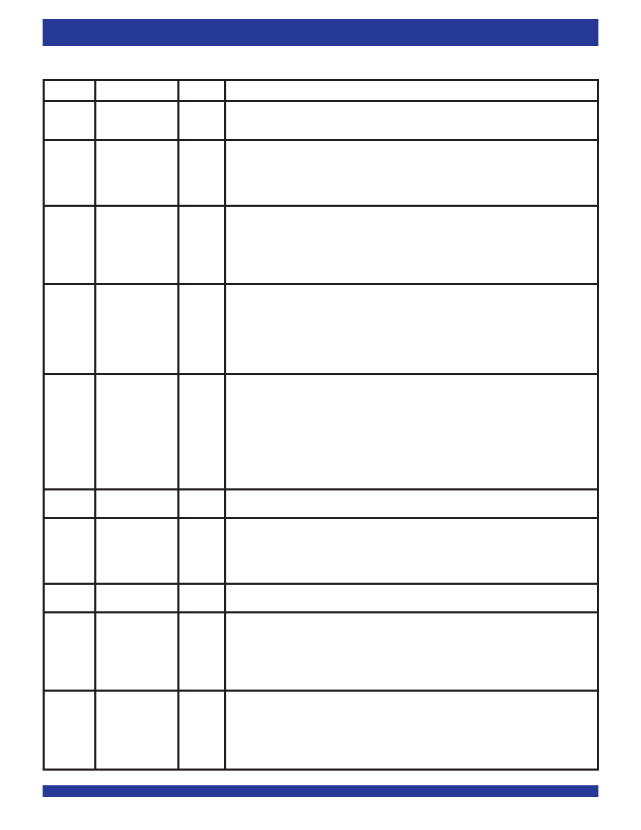
PIN DESCRIPTIONS (CONTINUED)
FSTR
PAFn Flag Bus
LVTTL
Polled operations has been selected, FSTR should be tied inactive, LOW. Note, that a
PAFn flag bus
(Continued) Strobe
INPUT
selectioncannotbemade,(FSTRmustNOTgoactive)untilprogrammingoftheparthasbeencompleted
and
SENO has gone LOW.
FSYNC
PAFn Bus Sync
LVTTL
FSYNC is an output from the multi-queue device that provides a synchronizing pulse for the
PAFn bus
OUTPUT
during Polled operation of the
PAFn bus. During Polled operation each quadrant of queue status flags
is loaded on to the
PAFn bus outputs sequentially based on WCLK. The first WCLK rising edge loads
device 1 on to the
PAFn bus outputs, the second WCLK rising edge loads device 2 and so on. During
the WCLKcycle that a selected device is placed on to the
PAFn bus, the FSYNC output will be HIGH.
FXI
PAFn Bus
LVTTL
The FXI input is used when multi-queue devices are connected in expansion mode and Polled
PAFn
Expansion In
INPUT
bus operation has been selected. FXI of device ‘N’ connects directly to FXO of device ‘N-1’. The FXI
receives a token from the previous device in a chain. In single device mode the FXI input must be tied
LOW if the
PAFnbusisoperatedindirectmode.IfthePAFnbusisoperatedinpolledmodetheFXIinput
must be connected to the FXO output of the same device. In expansion mode the FXI of the first device
should be tied LOW, when direct mode is selected.
FXO
PAFn Bus
LVTTL
FXO is an output that is used when multi-queue devices are connected in expansion mode and Polled
Expansion Out
OUTPUT
PAFnbusoperationhasbeenselected.FXOofdevice‘N’connectsdirectlytoFXIofdevice‘N+1’.This
pinpulsesHIGHwhendeviceNplacesits
PAFstatusontothePAFnbuswithrespecttoWCLK.Thispulse
(token) is then passed on to the next device in the chain ‘N+1’ and on the next WCLK rising edge the first
quadrant of device N+1 will be loaded on to the
PAFn bus. This continues through the chain and FXO
of the last device is then looped back to FXI of the first device. The FSYNC output of each device in the
chain provides synchronization to the user of this looping event.
ID[2:0](1)
Device ID Pins
LVTTL
For the 4Q multi-queue device the WRADD address bus is 5 bits and RDADD address bus is 6 bits wide.
INPUT
Whenaqueueselectiontakesplacethe3MSb’softhisaddressbusareusedtoaddressthespecificdevice
(the LSb’s are used to address the queue within that device). During write/read operations the 3 MSb’s
of the address are compared to the device ID pins. The first device in a chain of Multi-Queue’s (connected
in expansion mode), may be setup as ‘000’, the second as ‘001’ and so on through to device 8 which is
‘111’, however the ID does not have to match the device order. In single device mode these pins should
be setup as ‘000’ and the 3 MSb’s of the WRADD and RDADD address busses should be tied LOW. The
ID[2:0] inputs setup a respective devices ID during master reset. These ID pins must not toggle during
any device operation. Note, the device selected as the ‘Master’ does not have to have the ID of ‘000’.
IW(1)
InputWidth
LVTTL
ThispinisusedinconjunctionwithOWandBMtosetuptheinputandoutputbuswidthstobeacombination
INPUT
of x9, x18 or x36, (providing that one port is x36).
MAST(1)
Master Device
LVTTL
The state of this input at Master Reset determines whether a given device (within a chain of devices), is the
INPUT
MasterdeviceoraSlave.IfthispinisHIGH,thedeviceisthemaster,ifitisLOWthenitisaSlave.Themaster
device is the first to take control of all outputs after a master reset, all slave devices go to High-Impedance,
preventing bus contention. If a multi-queue device is being used in single device mode, this pin must
be set HIGH.
MRS
Master Reset
LVTTL
Amasterresetisperformedbytaking
MRSfromHIGHtoLOW,toHIGH.Deviceprogrammingisrequired
INPUT
aftermasterreset.
OE
OutputEnable
LVTTL
TheOutputenablesignalisanAsynchronoussignalusedtoprovidethree-statecontrolofthemulti-queue
INPUT
data output bus, Qout. If a device has been configured as a “Master” device, the Qout data outputs will
be in a Low Impedance condition if the
OEinputisLOW.IfOE isHIGHthentheQoutdataoutputswillbe
in High Impedance. If a device is configured a “Slave” device, then the Qout data outputs will always be
inHighImpedanceuntilthatdevicehasbeenselectedontheReadPort,atwhichpoint
OEprovidesthree-
state of that respective device.
OV
Output Valid Flag
LVTTL
Thisoutputflagprovidesoutputvalidstatusforthedatawordpresentonthemulti-queueflow-controldevice
OUTPUT
data output port, Qout. This flag is therefore, 2-stage delayed to match the data output path delay. That
is, there is a 2 RCLK cycle delay from the time a given queue is selected for reads, to the time the
OVflag
represents the data in that respective queue. When a selected queue on the read port is read to empty,
the
OV flag will go HIGH, indicating that data on the output bus is not valid. The OV flag also has High-
Impedance capability, required when multiple devices are used and the
OV flags are tied together.
Symbol
Name
I/O TYPE
Description
相关PDF资料 |
PDF描述 |
|---|---|
| LFXP6E-4Q208I | IC FPGA 5.8KLUTS 142I/O 208-PQFP |
| LFXP6C-5Q208C | IC FPGA 5.8KLUTS 142I/O 208-PQFP |
| LFXP6C-4Q208I | IC FPGA 5.8KLUTS 142I/O 208-PQFP |
| LFXP6E-4QN208I | IC FPGA 5.8KLUTS 208PQFP |
| LFXP6E-5QN208C | IC FPGA 5.8KLUTS 208PQFP |
相关代理商/技术参数 |
参数描述 |
|---|---|
| IDT72V51246L7-5BB | 功能描述:IC FLOW CTRL MULTI QUEUE 256-BGA RoHS:否 类别:集成电路 (IC) >> 专用 IC 系列:- 产品培训模块:Lead (SnPb) Finish for COTS Obsolescence Mitigation Program 标准包装:1 系列:- 类型:调帧器 应用:数据传输 安装类型:表面贴装 封装/外壳:400-BBGA 供应商设备封装:400-PBGA(27x27) 包装:散装 |
| IDT72V51246L7-5BB8 | 功能描述:IC FLOW CTRL MULTI QUEUE 256-BGA RoHS:否 类别:集成电路 (IC) >> 专用 IC 系列:- 产品培训模块:Lead (SnPb) Finish for COTS Obsolescence Mitigation Program 标准包装:1 系列:- 类型:调帧器 应用:数据传输 安装类型:表面贴装 封装/外壳:400-BBGA 供应商设备封装:400-PBGA(27x27) 包装:散装 |
| IDT72V51246L7-5BBI | 功能描述:IC FLOW CTRL MULTI QUEUE 256-BGA RoHS:否 类别:集成电路 (IC) >> 专用 IC 系列:- 产品培训模块:Lead (SnPb) Finish for COTS Obsolescence Mitigation Program 标准包装:1 系列:- 类型:调帧器 应用:数据传输 安装类型:表面贴装 封装/外壳:400-BBGA 供应商设备封装:400-PBGA(27x27) 包装:散装 |
| IDT72V51253L6BB | 功能描述:IC FLOW CTRL MULTI QUEUE 256-BGA RoHS:否 类别:集成电路 (IC) >> 专用 IC 系列:- 产品培训模块:Lead (SnPb) Finish for COTS Obsolescence Mitigation Program 标准包装:1 系列:- 类型:调帧器 应用:数据传输 安装类型:表面贴装 封装/外壳:400-BBGA 供应商设备封装:400-PBGA(27x27) 包装:散装 |
| IDT72V51253L6BB8 | 功能描述:IC FLOW CTRL MULTI QUEUE 256-BGA RoHS:否 类别:集成电路 (IC) >> 专用 IC 系列:- 产品培训模块:Lead (SnPb) Finish for COTS Obsolescence Mitigation Program 标准包装:1 系列:- 类型:调帧器 应用:数据传输 安装类型:表面贴装 封装/外壳:400-BBGA 供应商设备封装:400-PBGA(27x27) 包装:散装 |
发布紧急采购,3分钟左右您将得到回复。