- 您现在的位置:买卖IC网 > Datasheet目录443 > IRF6613 (International Rectifier)MOSFET N-CH 40V DIRECTFET-MT Datasheet资料下载
参数资料
| 型号: | IRF6613 |
| 厂商: | International Rectifier |
| 文件页数: | 1/9页 |
| 文件大小: | 0K |
| 描述: | MOSFET N-CH 40V DIRECTFET-MT |
| 标准包装: | 4,800 |
| 系列: | HEXFET® |
| FET 型: | MOSFET N 通道,金属氧化物 |
| FET 特点: | 逻辑电平门 |
| 漏极至源极电压(Vdss): | 40V |
| 电流 - 连续漏极(Id) @ 25° C: | 23A |
| 开态Rds(最大)@ Id, Vgs @ 25° C: | 3.4 毫欧 @ 23A,10V |
| Id 时的 Vgs(th)(最大): | 2.25V @ 250µA |
| 闸电荷(Qg) @ Vgs: | 63nC @ 4.5V |
| 输入电容 (Ciss) @ Vds: | 5950pF @ 15V |
| 功率 - 最大: | 2.8W |
| 安装类型: | 表面贴装 |
| 封装/外壳: | DirectFET? 等容 MT |
| 供应商设备封装: | DIRECTFET? MT |
| 包装: | 带卷 (TR) |
�� �
�
�PD� -� 95881B�
�IRF6613�
�l�
�l�
�l�
�l�
�l�
�l�
�l�
�Application� Specific� MOSFETs�
�Ideal� for� Synchronous� Rectification� in� Isolated�
�DC-DC� Converters�
�Low� Conduction� Losses�
�Low� Switching� Losses�
�Low� Profile� (<0.7� mm)�
�Dual� Sided� Cooling� Compatible�
�Compatible� with� existing� Surface� Mount� Techniques�
�V� DSS�
�40V�
�HEXFET� ?� Power� MOSFET�
�R� DS(on)� max� Qg(typ.)�
�3.4m� ?� @V� GS� =� 10V� 42nC�
�4.1m� ?� @V� GS� =� 4.5V�
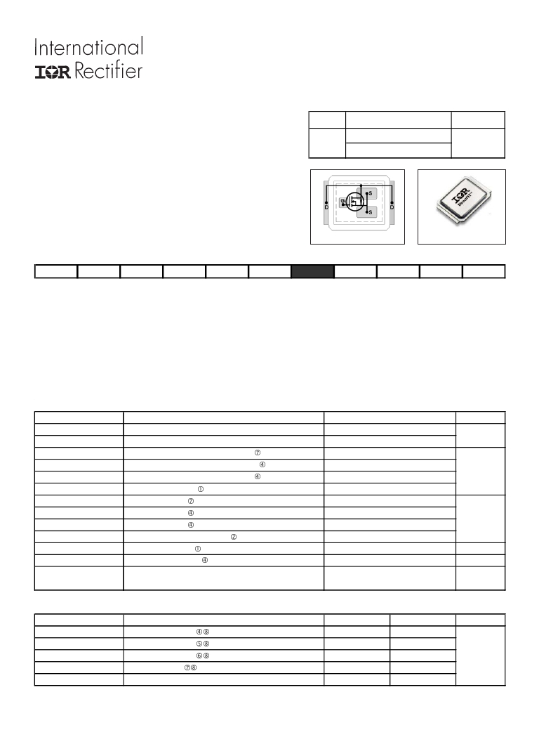
�DirectFET� ?� ISOMETRIC�
�MT�
�Applicable� DirectFET� Outline� and� Substrate� Outline� (see� p.8,9� for� details)�
�SQ�
�SX�
�ST�
�MQ�
�MX�
�MT�
�Description�
�The� IRF6613� combines� the� latest� HEXFET?� Power� MOSFET� Silicon� technology� with� the� advanced� DirectFET� TM� packaging� to� achieve� the�
�lowest� on-state� resistance� in� a� package� that� has� the� footprint� of� an� SO-8� and� only� 0.7� mm� profile.� The� DirectFET� package� is� compatible� with�
�existing� layout� geometries� used� in� power� applications,� PCB� assembly� equipment� and� vapor� phase,� infra-red� or� convection� soldering� techniques,�
�when� application� note� AN-1035� is� followed� regarding� the� manufacturing� methods� and� processes.� The� DirectFET� package� allows� dual� sided�
�cooling� to� maximize� thermal� transfer� in� power� systems,� IMPROVING� previous� best� thermal� resistance� by� 80%.�
�The� IRF6613� balances� both� low� resistance� and� low� charge� along� with� ultra� low� package� inductance� to� reduce� both� conduction� and� switching�
�losses.� The� reduced� total� losses� make� this� product� ideal� for� high� efficiency� DC-DC� converters� that� power� the� latest� generation� of� processors�
�operating� at� higher� frequencies.� The� IRF6613� has� been� optimized� for� parameters� that� are� critical� in� synchronous� buck� converters� including�
�Rds(on),� gate� charge� and� Cdv/dt-induced� turn� on� immunity.� The� IRF6613� offers� particularly� low� Rds(on)� and� high� Cdv/dt� immunity� for� synchro-�
�nous� FET� applications� .�
�Absolute� Maximum� Ratings�
�Parameter�
�Max.�
�Units�
�V� DS�
�V� GS�
�I� D� @� T� C� =� 25°C�
�I� D� @� T� A� =� 25°C�
�I� D� @� T� A� =� 70°C�
�I� DM�
�P� D� @T� C� =� 25°C�
�P� D� @T� A� =� 25°C�
�P� D� @T� A� =� 70°C�
�E� AS�
�I� AR�
�T� J�
�T� STG�
�Drain-to-Source� Voltage�
�Gate-to-Source� Voltage�
�Continuous� Drain� Current,� V� GS� @� 10V�
�Continuous� Drain� Current,� V� GS� @� 10V�
�Continuous� Drain� Current,� V� GS� @� 10V�
�Pulsed� Drain� Current�
�Power� Dissipation�
�Power� Dissipation�
�Power� Dissipation�
�Single� Pulse� Avalanche� Energy�
�Avalanche� Current�
�Linear� Derating� Factor�
�Operating� Junction� and�
�Storage� Temperature� Range�
�40�
�±20�
�150�
�23�
�18�
�180�
�89�
�2.8�
�1.8�
�200�
�18�
�0.022�
�-40� to� +� 150�
�V�
�A�
�W�
�mJ�
�A�
�W/°C�
�°C�
�Thermal� Resistance�
�Parameter�
�Typ.�
�Max.�
�Units�
�R� θ� JA�
�R� θ� JA�
�Junction-to-Ambient�
�Junction-to-Ambient�
�–––�
�12.5�
�45�
�–––�
�R� θ� JA�
�R� θ� JC�
�R� θ� J-PCB�
�Junction-to-Ambient�
�Junction-to-Case�
�Junction-to-PCB� Mounted�
�20�
�–––�
�1.0�
�–––�
�1.4�
�–––�
�°C/W�
�Notes� ?� through� ?� are� on� page� 2�
�www.irf.com�
�1�
�9/30/05�
�相关PDF资料 |
PDF描述 |
|---|---|
| IRF6614TR1 | MOSFET N-CH 40V DIRECTFET-ST |
| IRF6633TR1 | MOSFET N-CH 20V 16A DIRECTFET-MP |
| IRF6644TR1 | MOSFET N-CH 100V DIRECTFET-MN |
| IRF6645 | MOSFET N-CH 100V DIRECTFET-SJ |
| IRF6655TR1 | MOSFET N-CH 100V DIRECTFET-SH |
相关代理商/技术参数 |
参数描述 |
|---|---|
| IRF6613TR1 | 功能描述:MOSFET 40V N-CH HEXFET 3.4mOhms 42nC RoHS:否 制造商:STMicroelectronics 晶体管极性:N-Channel 汲极/源极击穿电压:650 V 闸/源击穿电压:25 V 漏极连续电流:130 A 电阻汲极/源极 RDS(导通):0.014 Ohms 配置:Single 最大工作温度: 安装风格:Through Hole 封装 / 箱体:Max247 封装:Tube |
| IRF6613TR1PBF | 功能描述:MOSFET MOSFT 40V 150A 3.4mOhm 42nC Qg RoHS:否 制造商:STMicroelectronics 晶体管极性:N-Channel 汲极/源极击穿电压:650 V 闸/源击穿电压:25 V 漏极连续电流:130 A 电阻汲极/源极 RDS(导通):0.014 Ohms 配置:Single 最大工作温度: 安装风格:Through Hole 封装 / 箱体:Max247 封装:Tube |
| IRF6613TR1PBF | 制造商:International Rectifier 功能描述:MOSFET |
| IRF6613TRPBF | 功能描述:MOSFET 40V N-CH HEXFET 3.4mOhms 42nC RoHS:否 制造商:STMicroelectronics 晶体管极性:N-Channel 汲极/源极击穿电压:650 V 闸/源击穿电压:25 V 漏极连续电流:130 A 电阻汲极/源极 RDS(导通):0.014 Ohms 配置:Single 最大工作温度: 安装风格:Through Hole 封装 / 箱体:Max247 封装:Tube |
| IRF6614 | 功能描述:MOSFET 40V 1 N-CH 5.9mOhm DirectFET 1.8Vgs RoHS:否 制造商:STMicroelectronics 晶体管极性:N-Channel 汲极/源极击穿电压:650 V 闸/源击穿电压:25 V 漏极连续电流:130 A 电阻汲极/源极 RDS(导通):0.014 Ohms 配置:Single 最大工作温度: 安装风格:Through Hole 封装 / 箱体:Max247 封装:Tube |
发布紧急采购,3分钟左右您将得到回复。