参数资料
| 型号: | ISL6308CRZ |
| 厂商: | Intersil |
| 文件页数: | 18/28页 |
| 文件大小: | 0K |
| 描述: | IC CTRLR PWM 3PHASE BUCK 40-QFN |
| 标准包装: | 500 |
| 应用: | 控制器,DDR |
| 输入电压: | 5 V ~ 12 V |
| 输出数: | 1 |
| 输出电压: | 0.6 V ~ 2.3 V |
| 工作温度: | 0°C ~ 70°C |
| 安装类型: | 表面贴装 |
| 封装/外壳: | 40-VFQFN 裸露焊盘 |
| 供应商设备封装: | 40-QFN(6x6) |
| 包装: | 管件 |
第1页第2页第3页第4页第5页第6页第7页第8页第9页第10页第11页第12页第13页第14页第15页第16页第17页当前第18页第19页第20页第21页第22页第23页第24页第25页第26页第27页第28页
�� �
�
�ISL6308�
�the� lower� MOSFET� is� due� to� current� conducted� through� the�
�channel� resistance� (r� DS(ON)� ).� In� Equation� 14,� I� M� is� the�
�maximum� continuous� output� current,� I� PP� is� the� peak-to-peak�
�OUTPUT� CURRENT�
�inductor� current� (see� Equation� 1),� and� d� is� the� duty� cycle�
�(V� OUT� /V� IN� ).�
�·� ?� I� M� ?� 2� I� L� ,� PP� ?� (� 1� –� d� )�
�P� LOW� ,� 1� =� r� DS� (� ON� )� ?� ?� ------� ?� ?� (� 1� –� d� )� +� -------------------------------------�
�0A�
�?� N� ?� 12�
�(EQ.� 14)�
�An� additional� term� can� be� added� to� the� lower-MOSFET� loss�
�equation� to� account� for� additional� loss� accrued� during� the� dead�
�P� LOW� ,� 2� =� V� D� (� ON� )� ?� F� SW� ?� ?� ------� +� ---------� ?� ?� t� d1� +� ?� ------� –� ---------� ?� ?� t� d2�
�OUTPUT� VOLTAGE�
�0V�
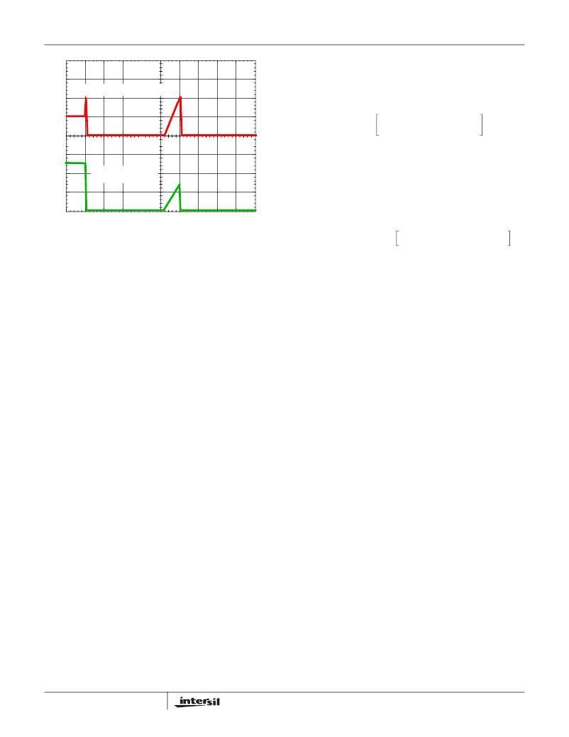
�FIGURE� 14.� OVERCURRENT� BEHAVIOR� IN� HICCUP� MODE�
�General� Design� Guide�
�This� design� guide� is� intended� to� provide� a� high-level�
�explanation� of� the� steps� necessary� to� create� a� multi-phase�
�power� converter.� It� is� assumed� that� the� reader� is� familiar� with�
�many� of� the� basic� skills� and� techniques� referenced� in� the�
�following.� In� addition� to� this� guide,� Intersil� provides� complete�
�reference� designs� that� include� schematics,� bills� of� materials,�
�and� example� board� layouts� for� many� applications.�
�Power� Stages�
�The� first� step� in� designing� a� multi-phase� converter� is� to�
�determine� the� number� of� phases.� This� determination�
�depends� heavily� on� the� cost� analysis� which� in� turn� depends�
�on� system� constraints� that� differ� from� one� design� to� the� next.�
�Principally,� the� designer� will� be� concerned� with� whether�
�components� can� be� mounted� on� both� sides� of� the� circuit�
�board,� whether� through-hole� components� are� permitted,� the�
�total� board� space� available� for� power-supply� circuitry,� and�
�the� maximum� amount� of� load� current.� Generally� speaking,�
�the� most� economical� solutions� are� those� in� which� each�
�phase� handles� between� 25A� and� 30A.� All� surface-mount�
�designs� will� tend� toward� the� lower� end� of� this� current� range.�
�If� through-hole� MOSFETs� and� inductors� can� be� used,� higher�
�time� when� inductor� current� is� flowing� through� the� lower-�
�MOSFET� body� diode.� This� term� is� dependent� on� the� diode�
�forward� voltage� at� I� M� ,� V� D(ON)� ,� the� switching� frequency,� F� SW� ,�
�and� the� length� of� dead� times,� t� d1� and� t� d2� ,� at� the� beginning� and�
�the� end� of� the� lower-MOSFET� conduction� interval� respectively.�
�I� M� I� PP� I� M� I� PP�
�?� N� 2� ?� ?� N� 2� ?�
�(EQ.� 15)�
�The� total� maximum� power� dissipated� in� each� lower� MOSFET�
�is� approximated� by� the� summation� of� P� LOW,1� and� P� LOW,2� .�
�UPPER� MOSFET� POWER� CALCULATION�
�In� addition� to� r� DS(ON)� losses,� a� large� portion� of� the� upper�
�MOSFET� losses� are� due� to� currents� conducted� across� the�
�input� voltage� (V� IN� )� during� switching.� Since� a� substantially�
�higher� portion� of� the� upper-MOSFET� losses� are� dependent� on�
�switching� frequency,� the� power� calculation� is� more� complex.�
�Upper� MOSFET� losses� can� be� divided� into� separate�
�components� involving� the� upper� MOSFET� switching� times,�
�the� lower-MOSFET� body-diode� reverse� recovery� charge,� Q� rr� ,�
�and� the� upper� MOSFET� r� DS(ON)� conduction� loss.�
�When� the� upper� MOSFET� turns� off,� the� lower� MOSFET� does�
�not� conduct� any� portion� of� the� inductor� current� until� the�
�voltage� at� the� phase� node� falls� below� ground.� Once� the�
�lower� MOSFET� begins� conducting,� the� current� in� the� upper�
�MOSFET� falls� to� zero� as� the� current� in� the� lower� MOSFET�
�ramps� up� to� assume� the� full� inductor� current.� In� Equation� 16,�
�the� required� time� for� this� commutation� is� t� 1� and� the�
�approximated� associated� power� loss� is� P� UP,1� .�
�I� M�
�I� PP�
�P� UP� ,� 1� ≈� V� IN� ?� ?� ------� +� ---------� ?� ?� ?� ----� 1� ?� ?� F� SW�
�per-phase� currents� are� possible.� In� cases� where� board�
�space� is� the� limiting� constraint,� current� can� be� pushed� as�
�high� as� 40A� per� phase,� but� these� designs� require� heat� sinks�
�?� N� 2� ?� ?� 2� ?�
�?� t� ?�
�(EQ.� 16)�
�and� forced� air� to� cool� the� MOSFETs,� inductors� and� heat�
�dissipating� surfaces.�
�MOSFETs�
�At� turn� on,� the� upper� MOSFET� begins� to� conduct� and� this�
�transition� occurs� over� a� time� t� 2� .� In� Equation� 17,� the�
�approximate� power� loss� is� P� UP,2� .�
�P� UP� ,� 2� ≈� V� IN� ?� ?� ------� –� ---------� ?�
�?� ?� ----� 2� ?� ?� F� SW�
�The� choice� of� MOSFETs� depends� on� the� current� each�
�MOSFET� will� be� required� to� conduct,� the� switching� frequency,�
�?� I� M� I� PP� ?�
�?� N� 2� ?�
�?� t� ?�
�?� 2� ?�
�(EQ.� 17)�
�the� capability� of� the� MOSFETs� to� dissipate� heat,� and� the�
�availability� and� nature� of� heat� sinking� and� air� flow.�
�LOWER� MOSFET� POWER� CALCULATION�
�The� calculation� for� the� approximate� power� loss� in� the� lower�
�MOSFET� can� be� simplified,� since� virtually� all� of� the� loss� in�
�18�
�A� third� component� involves� the� lower� MOSFET� reverse�
�recovery� charge,� Q� rr� .� Since� the� inductor� current� has� fully�
�commutated� to� the� upper� MOSFET� before� the� lower�
�MOSFET� body� diode� can� recover� all� of� Q� rr� ,� it� is� conducted�
�FN9208.4�
�September� 30,� 2008�
�相关PDF资料 |
PDF描述 |
|---|---|
| ACM18DRSN-S288 | CONN EDGECARD EXTEND 36POS 0.156 |
| RCM22DTAD-S189 | CONN EDGECARD 44POS R/A .156 SLD |
| MAX8860EUA28+ | IC REG LDO 2.82V/ADJ .3A 8-UMAX |
| 2512-562K | INDUCTOR POWER 5.6UH MOLDED SMD |
| ACM18DRSH-S288 | CONN EDGECARD EXTEND 36POS 0.156 |
相关代理商/技术参数 |
参数描述 |
|---|---|
| ISL6308CRZR5374 | 制造商:Intersil Corporation 功能描述:ISL6308CRZ W/ 24HR BURN-IN - Rail/Tube 制造商:Intersil Corporation 功能描述:IC CTRLR PWM 3PHASE BUCK 40-QFN 制造商:Intersil 功能描述:ISL6308CRZ W/24HRU RN-IN |
| ISL6308CRZ-T | 功能描述:电压模式 PWM 控制器 DAC-LESS MULTI-PHS PWM CNTRLR W/3-DRVRS RoHS:否 制造商:Texas Instruments 输出端数量:1 拓扑结构:Buck 输出电压:34 V 输出电流: 开关频率: 工作电源电压:4.5 V to 5.5 V 电源电流:600 uA 最大工作温度:+ 125 C 最小工作温度:- 40 C 封装 / 箱体:WSON-8 封装:Reel |
| ISL6308CRZ-TR5374 | 制造商:Intersil Corporation 功能描述:ISL6308CRZ W/ 24HR BURN-IN - Tape and Reel 制造商:Intersil Corporation 功能描述:IC CTRLR PWM 3PHASE BUCK 40-QFN 制造商:Intersil 功能描述:ISL6308CRZ W/24HRU RN-IN |
| ISL6308CRZ-TR5453 | 制造商:Intersil Corporation 功能描述:STD. ISL6308CRZ-T W/GOLD BOND WIRE ONLY - Tape and Reel |
| ISL6308EVAL1Z | 制造商:Intersil Corporation 功能描述:ISL6308 EVALUATION BOARD 1 - ROHS COMPLIANT - QFN - Bulk |
发布紧急采购,3分钟左右您将得到回复。