参数资料
| 型号: | ISL8120IRZEC |
| 厂商: | Intersil |
| 文件页数: | 24/33页 |
| 文件大小: | 0K |
| 描述: | IC REG CTRLR BUCK PWM VM 32-QFN |
| 标准包装: | 60 |
| PWM 型: | 电压模式 |
| 输出数: | 2 |
| 频率 - 最大: | 1.5MHz |
| 占空比: | 90% |
| 电源电压: | 3 V ~ 22 V |
| 降压: | 是 |
| 升压: | 无 |
| 回扫: | 无 |
| 反相: | 无 |
| 倍增器: | 无 |
| 除法器: | 无 |
| Cuk: | 无 |
| 隔离: | 无 |
| 工作温度: | -40°C ~ 85°C |
| 封装/外壳: | 32-VFQFN 裸露焊盘 |
| 包装: | 管件 |
第1页第2页第3页第4页第5页第6页第7页第8页第9页第10页第11页第12页第13页第14页第15页第16页第17页第18页第19页第20页第21页第22页第23页当前第24页第25页第26页第27页第28页第29页第30页第31页第32页第33页
�� �
�
�ISL8120IR�
�VMON1�
�113%�
�To� protect� the� overall� power� trains� in� case� of� only� one�
�channel� of� a� multiphase� system� detecting� OV,� the� low-side�
�87%�
�EN/FF1�
�VMON1>120%�
�VMON2�
�OR�
�multiphase�
�MODE� =� HIGH�
�OR�
�AND�
�AND�
�FORCE�
�LGATE1�
�HIGH�
�MOSFET� always� turns� on� at� the� conditions� of� EN/FF� =� LOW�
�and� the� output� voltage� above� 113%� (all� VMON� pins� and� EN�
�pins� are� tied� together)� and� turns� off� after� the� output� drops�
�below� 87%.� Thus,� in� a� high� phase� count� application�
�(Multiphase� Mode),� all� cascaded� ICs� can� latch� off�
�simultaneously� via� EN� pins,� and� each� IC� shares� the� same�
�sink� current� to� reduce� the� stress� and� eliminate� the� bouncing�
�113%�
�among� phases.�
�87%�
�EN/FF2�
�OR�
�AND�
�FORCE�
�LGATE2�
�HIGH�
�VOUT�
�120%�
�VMON2>120%�
�3� CYCLES�
�3� CYCLES�
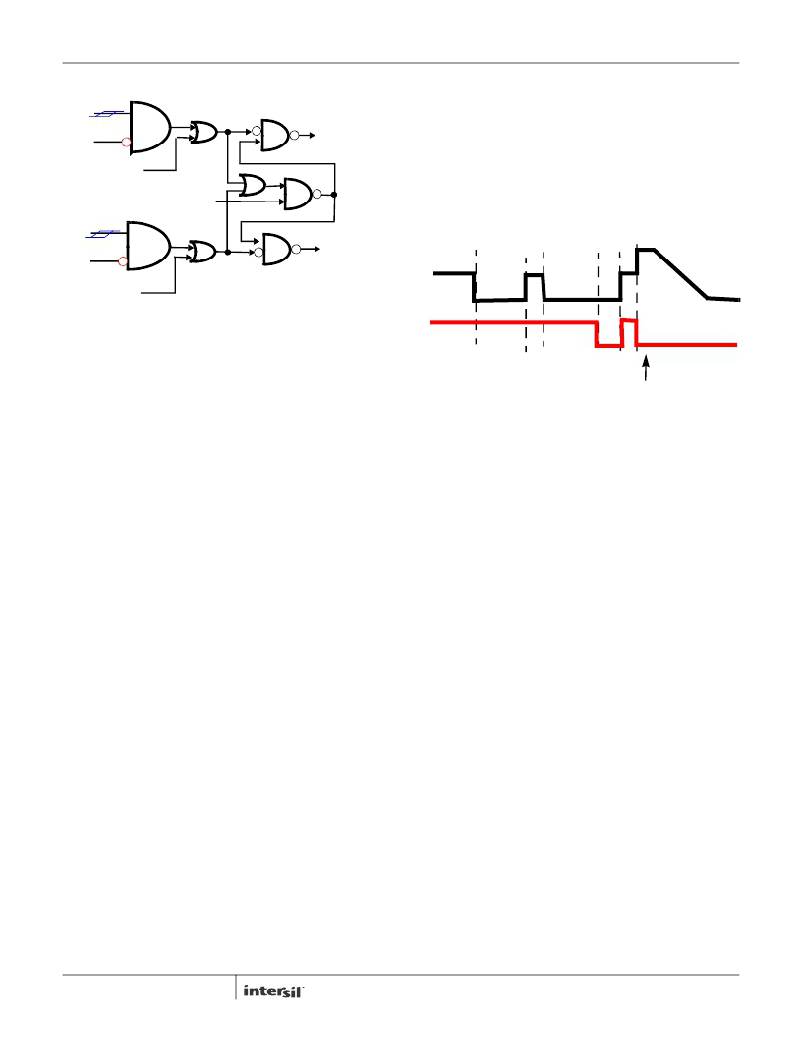
�FIGURE� 11.� FORCE� LGATE� HIGH� LOGIC�
�PGOOD�
�UV�
�OV� LATCH�
�Both� channels� share� the� same� PGOOD� output.� Either� of� the�
�channels� indicating� out-of-regulation� will� pull-down� the�
�PGOOD� pin.� The� Power-Good� comparators� monitor� the�
�voltage� on� the� VMON� pins.� The� trip� points� are� shown� in�
�Figure� 10.� PGOOD� will� not� be� asserted� until� after� the�
�completion� of� the� soft-start� cycle� of� both� channels.� If�
�Channels� 1� or� 2� are� not� used,� the� Power-Good� can� stay� in�
�operation� by� connecting� 2� channels’� VMON� pins� together.�
�The� PGOOD� pulls� low� upon� both� EN/FF’s� disabling� it� if� one�
�of� the� VMON� pins’� voltage� is� out� of� the� threshold� window.�
�PGOOD� will� not� pull� low� until� the� fault� presents� for� three�
�consecutive� clock� cycles.� In� Dual/DDR� application,� if� the�
�turn-off� channel� pre-charges� its� VMON� within� the� PGOOD�
�threshold� window,� it� could� indicate� Power-Good,� however,�
�the� PGOOD� signal� can� pull� low� with� an� external� PNP� or�
�PMOS� transistor� via� the� EN/FF� of� the� corresponding� off�
�channel.�
�Undervoltage� and� Overvoltage� Protection�
�The� Undervoltage� (UV)� and� Overvoltage� (OV)� protection�
�circuitry� monitor� the� voltage� on� the� VMON� pins.� The� UV�
�functionality� is� not� enabled� until� the� end� of� soft-start.� An� OV�
�condition� (>120%)� during� soft-start� would� latch� IC� off.�
�In� an� UV� event,� if� the� output� drops� below� -13%� (-9%� is� the�
�hysteresis� level)� due� to� some� reasons� other� than� OV,� OC,�
�OT,� and� PLL� faults� (EN/FF� is� not� pulled� low)� of� the� target�
�level� at� the� output� voltage� falling� edge,� the� lower� MOSFETs�
�will� turn� off� to� avoid� any� negative� voltage� ringing.�
�An� OV� event� (V� OUT� >� 120%)� causes� the� high-side� MOSFET�
�to� latch� off� permanently,� while� the� low-side� MOSFET� turns�
�on� and� then� turns� off� after� the� output� voltage� drops� below�
�87%.� At� the� same� time,� the� EN/FF� and� PGOOD� are� also�
�latched� low.� The� latch� condition� can� be� reset� only� by�
�recycling� VCC.� In� Dual/DDR� mode,� each� channel� is�
�responsible� for� its� own� OV� event� with� the� corresponding�
�VMON� as� the� monitor.� In� multiphase� mode,� both� channels�
�respond� simultaneously� when� either� triggers� an� OV� event.�
�24�
�UGATE� AND� EN/FF� LATCH� LOW�
�FIGURE� 12.� UV� AND� OV� TIMING� DIAGRAM�
�PRE-POR� Overvoltage� Protection� (PRE-POR-OVP)�
�When� both� the� VCC� and� PVCC� are� below� PORs� (not� include�
�EN� POR),� the� UGATE� is� low� and� LGATE� is� floating� (high�
�impedance).� EN/FF� has� no� control� on� LGATE� when� below�
�PORs.� When� above� PORs,� the� LGATE� would� not� be� floating�
�but� toggling� with� its� PWM� pulses.� An� external� 10� Ω� resistor,�
�connected� in� between� Phase� and� LGATE� nodes,� enables�
�the� PRE-POR-OVP� circuit.� The� output� of� the� converter� that�
�is� equal� to� phase� node� voltage� via� output� inductors� is� then�
�effectively� clamped� to� the� low-side� MOSFET’s� gate�
�threshold� voltage,� which� provides� some� protection� to� the�
�microprocessor� if� the� upper� MOSFET(s)� is� shorted� during�
�start-up,� shutdown,� or� normal� operations.� For� complete�
�protection,� the� low-side� MOSFET� should� have� a� gate�
�threshold� that� is� much� smaller� than� the� maximum� voltage�
�rating� of� the� load.�
�The� PRE-POR-OVP� works� against� pre-biased� start-up� when�
�pre-charged� output� voltage� is� higher� than� the� threshold� of�
�the� low-side� MOSFET,� however,� it� can� be� disabled� by�
�placing� a� 2k� resistor� from� LGATE� to� ground.�
�Over-Temperature� Protection� (OTP)�
�When� the� junction� temperature� of� the� IC� is� greater� than�
�+150°C� (typically),� both� EN/FF� pins� pull� low� to� inform� other�
�cascaded� channels� via� their� EN/FF� pins.� All� connected�
�EN/FFs� stay� low� and� release� after� the� IC’s� junction�
�temperature� drops� below� +125°C� (typically),� with� a� +25°C�
�hysteresis� (typical).�
�FN6763.2�
�November� 11,� 2011�
�相关PDF资料 |
PDF描述 |
|---|---|
| ISL8120IRZ | IC REG CTRLR BUCK PWM VM 32-QFN |
| ISL8121IRZ | IC REG CTRLR BUCK PWM VM 24-QFN |
| ISL8126IRZ | IC REG CTRLR BUCK PWM VM 32-QFN |
| ISL8130IAZ | IC REG CTRLR BST FLYBK VM 20QSOP |
| ISL85001IRZ-T | IC REG BUCK ADJ 1A 12DFN |
相关代理商/技术参数 |
参数描述 |
|---|---|
| ISL8120IRZ-T | 功能描述:IC REG CTRLR BUCK PWM VM 32-QFN RoHS:是 类别:集成电路 (IC) >> PMIC - 稳压器 - DC DC 切换控制器 系列:- 产品培训模块:Lead (SnPb) Finish for COTS Obsolescence Mitigation Program 标准包装:2,500 系列:- PWM 型:电流模式 输出数:1 频率 - 最大:275kHz 占空比:50% 电源电压:18 V ~ 110 V 降压:无 升压:无 回扫:无 反相:无 倍增器:无 除法器:无 Cuk:无 隔离:是 工作温度:-40°C ~ 85°C 封装/外壳:8-SOIC(0.154",3.90mm 宽) 包装:带卷 (TR) |
| ISL8120IRZ-TEC | 功能描述:IC REG CTRLR BUCK PWM VM 32-QFN RoHS:是 类别:集成电路 (IC) >> PMIC - 稳压器 - DC DC 切换控制器 系列:- 产品培训模块:Lead (SnPb) Finish for COTS Obsolescence Mitigation Program 标准包装:2,500 系列:- PWM 型:电流模式 输出数:1 频率 - 最大:275kHz 占空比:50% 电源电压:18 V ~ 110 V 降压:无 升压:无 回扫:无 反相:无 倍增器:无 除法器:无 Cuk:无 隔离:是 工作温度:-40°C ~ 85°C 封装/外壳:8-SOIC(0.154",3.90mm 宽) 包装:带卷 (TR) |
| ISL8120IRZ-TK | 功能描述:IC REG CTRLR BUCK PWM VM 32-QFN RoHS:是 类别:集成电路 (IC) >> PMIC - 稳压器 - DC DC 切换控制器 系列:- 产品培训模块:Lead (SnPb) Finish for COTS Obsolescence Mitigation Program 标准包装:2,500 系列:- PWM 型:电流模式 输出数:1 频率 - 最大:275kHz 占空比:50% 电源电压:18 V ~ 110 V 降压:无 升压:无 回扫:无 反相:无 倍增器:无 除法器:无 Cuk:无 隔离:是 工作温度:-40°C ~ 85°C 封装/外壳:8-SOIC(0.154",3.90mm 宽) 包装:带卷 (TR) |
| ISL8121 | 制造商:INTERSIL 制造商全称:Intersil Corporation 功能描述:3V to 20V, Two-Phase Buck PWM Controller with Integrated 4A MOSFET Drivers |
| ISL8121EVAL1 | 制造商:INTERSIL 制造商全称:Intersil Corporation 功能描述:3V to 20V, Two-Phase Buck PWM Controller with Integrated 4A MOSFET Drivers |
发布紧急采购,3分钟左右您将得到回复。