- 您现在的位置:买卖IC网 > PDF目录17136 > KIT912F634EVME (Freescale Semiconductor)KIT EVAL FOR MM912F634 PDF资料下载
参数资料
| 型号: | KIT912F634EVME |
| 厂商: | Freescale Semiconductor |
| 文件页数: | 13/339页 |
| 文件大小: | 0K |
| 描述: | KIT EVAL FOR MM912F634 |
| 标准包装: | 1 |
| 类型: | MCU |
| 适用于相关产品: | MM912F634 |
| 所含物品: | 板,线缆,CD |
第1页第2页第3页第4页第5页第6页第7页第8页第9页第10页第11页第12页当前第13页第14页第15页第16页第17页第18页第19页第20页第21页第22页第23页第24页第25页第26页第27页第28页第29页第30页第31页第32页第33页第34页第35页第36页第37页第38页第39页第40页第41页第42页第43页第44页第45页第46页第47页第48页第49页第50页第51页第52页第53页第54页第55页第56页第57页第58页第59页第60页第61页第62页第63页第64页第65页第66页第67页第68页第69页第70页第71页第72页第73页第74页第75页第76页第77页第78页第79页第80页第81页第82页第83页第84页第85页第86页第87页第88页第89页第90页第91页第92页第93页第94页第95页第96页第97页第98页第99页第100页第101页第102页第103页第104页第105页第106页第107页第108页第109页第110页第111页第112页第113页第114页第115页第116页第117页第118页第119页第120页第121页第122页第123页第124页第125页第126页第127页第128页第129页第130页第131页第132页第133页第134页第135页第136页第137页第138页第139页第140页第141页第142页第143页第144页第145页第146页第147页第148页第149页第150页第151页第152页第153页第154页第155页第156页第157页第158页第159页第160页第161页第162页第163页第164页第165页第166页第167页第168页第169页第170页第171页第172页第173页第174页第175页第176页第177页第178页第179页第180页第181页第182页第183页第184页第185页第186页第187页第188页第189页第190页第191页第192页第193页第194页第195页第196页第197页第198页第199页第200页第201页第202页第203页第204页第205页第206页第207页第208页第209页第210页第211页第212页第213页第214页第215页第216页第217页第218页第219页第220页第221页第222页第223页第224页第225页第226页第227页第228页第229页第230页第231页第232页第233页第234页第235页第236页第237页第238页第239页第240页第241页第242页第243页第244页第245页第246页第247页第248页第249页第250页第251页第252页第253页第254页第255页第256页第257页第258页第259页第260页第261页第262页第263页第264页第265页第266页第267页第268页第269页第270页第271页第272页第273页第274页第275页第276页第277页第278页第279页第280页第281页第282页第283页第284页第285页第286页第287页第288页第289页第290页第291页第292页第293页第294页第295页第296页第297页第298页第299页第300页第301页第302页第303页第304页第305页第306页第307页第308页第309页第310页第311页第312页第313页第314页第315页第316页第317页第318页第319页第320页第321页第322页第323页第324页第325页第326页第327页第328页第329页第330页第331页第332页第333页第334页第335页第336页第337页第338页第339页
Electrical Characteristics
General
MM912F634
Freescale Semiconductor
11
3
Electrical Characteristics
3.1
General
This supplement contains electrical information for the embedded MC9S12I32 microcontroller die, as well as the MM912F634
analog die.
3.2
Absolute Maximum Ratings
Absolute maximum ratings are stress ratings only. A functional operation under or outside those maxima is not guaranteed.
Stress beyond those limits may affect the reliability or cause permanent damage of the device.
This device contains circuitry protecting against damage due to high static voltage or electrical fields. However, it is advised that
normal precautions be taken to avoid application of any voltages higher than maximum-rated voltages to this high-impedance
circuit. Reliability of operation is enhanced if unused inputs are tied to an appropriate voltage level. All voltages are with respect
to ground unless otherwise noted.
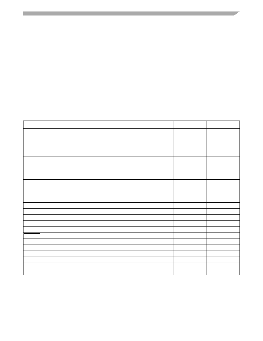
Table 5. Absolute Maximum Electrical Ratings - Analog Die
Ratings
Symbol
Value
Unit
Supply Voltage at VS1 and VS2
Normal Operation (DC)
Transient Conditions (load dump)
Transient input voltage with external component (according to LIN
Conformance Test Specification / ISO7637-2)
VSUP(SS)
VSUP(PK)
VSUP(TR)
-0.3 to 27
-0.3 to 40
see Section 3.9,
V
L0…L5 - Pin Voltage
Normal Operation with a series RLX resistor (DC)
Transient input voltage with external component (according to LIN
Conformance Test Specification / ISO7637-2)
VLxDC
VLxTR
-27 to 40
see Section 3.9,
V
LIN Pin Voltage
Normal Operation (DC)
Transient input voltage with external component (according to LIN
Conformance Test Specification / ISO7637-2)
VBUSDC
VBUSTR
-33 to 40
see Section 3.9,
V
Supply Voltage at VDDX
VDDX
-0.3 to 5.5
V
Supply Voltage at VDD (6)
VDD
-0.3 to 2.75
V
VDD output current
IVDD
Internally Limited
A
VDDX output current
IVDDX
Internally Limited
A
TCLK Pin Voltage
VTCLK
-0.3 to 10
V
RESET_A Pin Voltage
VIN
-0.3 to VDDx+0.3
V
Input / Output Pins PTB[0:2] Voltage
VIN
-0.3 to VDDx+0.3
V
HS1 and HS2 Pin Voltage (DC)
VHS
-0.3 to VS2+0.3
V
LS1 and LS2 Pin Voltage (DC)
VLS
-0.3 to 45
V
ISENSEH and ISENSEL Pin Voltage (DC)
VISENSE
-0.3 to 40
V
HSUP Pin Voltage (DC)
VHSUP
-0.3 to VS1+0.3
V
VSENSE Pin Voltage (DC)
VVSENSE
-27 to 40
V
Note:
6. Caution: As this pin is adjacent to the VDDX pin, care should be taken to avoid a short between VDD and VDDX, for example, during
the soldering process. A short-circuit between these pins might lead to permanent damage.
相关PDF资料 |
PDF描述 |
|---|---|
| MRJ0800DD-A | C/A MRJ21/MRJ21 GBE STRT CMR 80M |
| VE-JWF-EZ | CONVERTER MOD DC/DC 72V 25W |
| EBC28DCMD-S288 | CONN EDGECARD 56POS .100 EXTEND |
| RS-4805DZ/H3 | CONV DC/DC 2W 18-72VIN +/-05VOUT |
| 38S801C | INDUCTOR 0.80UH 12.5A SMD |
相关代理商/技术参数 |
参数描述 |
|---|---|
| KIT912H634EVME | 功能描述:开发板和工具包 - S08 / S12 DUAL LOW&HIDE SWITCH EVB RoHS:否 产品:Development Kits 工具用于评估:MC9S12G128 核心:S12 接口类型:CAN, LIN, RS-232, USB 工作电源电压:5 V 制造商:Freescale Semiconductor |
| KIT912J637EVME | 功能描述:电源管理IC开发工具 BATTERY SENSOR 912J637 RoHS:否 制造商:Maxim Integrated 产品:Evaluation Kits 类型:Battery Management 工具用于评估:MAX17710GB 输入电压: 输出电压:1.8 V |
| KIT912S812ECUEVM | 功能描述:电源管理IC开发工具 Single Cylinder S12XS E RoHS:否 制造商:Maxim Integrated 产品:Evaluation Kits 类型:Battery Management 工具用于评估:MAX17710GB 输入电压: 输出电压:1.8 V |
| Kit-916 | 制造商:ANDERSON POWER PRODUCTS 功能描述:KIT |
| Kit-917 | 制造商:ANDERSON POWER PRODUCTS 功能描述:KIT |
发布紧急采购,3分钟左右您将得到回复。