- 您现在的位置:买卖IC网 > PDF目录15309 > LTC1735CGN-1#TRPBF (Linear Technology)IC REG CTRLR BUCK PWM CM 16-SSOP PDF资料下载
参数资料
| 型号: | LTC1735CGN-1#TRPBF |
| 厂商: | Linear Technology |
| 文件页数: | 19/28页 |
| 文件大小: | 0K |
| 描述: | IC REG CTRLR BUCK PWM CM 16-SSOP |
| 标准包装: | 2,500 |
| PWM 型: | 电流模式 |
| 输出数: | 1 |
| 频率 - 最大: | 335kHz |
| 占空比: | 99.4% |
| 电源电压: | 3.5 V ~ 30 V |
| 降压: | 是 |
| 升压: | 无 |
| 回扫: | 无 |
| 反相: | 无 |
| 倍增器: | 无 |
| 除法器: | 无 |
| Cuk: | 无 |
| 隔离: | 无 |
| 工作温度: | 0°C ~ 85°C |
| 封装/外壳: | 16-SSOP(0.154",3.90mm 宽) |
| 包装: | 带卷 (TR) |
第1页第2页第3页第4页第5页第6页第7页第8页第9页第10页第11页第12页第13页第14页第15页第16页第17页第18页当前第19页第20页第21页第22页第23页第24页第25页第26页第27页第28页
�� �
�
�LTC1735-1�
�APPLICATIO� S� I� FOR� ATIO�
�Table� 1�
�and� control� currents.� V� IN� current� results� in� a� small�
�PGOOD� PIN�
�DC� Voltage:� 0V� to� 0.7V�
�Resistor� Pull-Up� to�
�INT� VCC� (or� Other� DC�
�Voltage� Less� Than� INTV� CC� )�
�Resistor� to� Ext� Clock:�
�(0V� to� 1.5V)�
�CONDITION�
�No� Power� Good� Indication�
�Burst� Mode� Operation� Disabled/Forced�
�Continuous� Current� Reversal� Enabled�
�Power� Good� Indication�
�Burst� Mode,� No� Current� Reversal�
�When� Power� is� Good�
�No� Power� Good� Indication�
�Burst� Mode� Operation� Disabled�
�(<� 0.1%)� loss� that� increases� with� V� IN� .�
�2.� INTV� CC� current� is� the� sum� of� the� MOSFET� driver� and�
�control� currents.� The� MOSFET� driver� current� results�
�from� switching� the� gate� capacitance� of� the� power�
�MOSFETs.� Each� time� a� MOSFET� gate� is� switched� from�
�low� to� high� to� low� again,� a� packet� of� charge� dQ� moves�
�from� INTV� CC� to� ground.� The� resulting� dQ/dt� is� a� current�
�No� Current� Reversal�
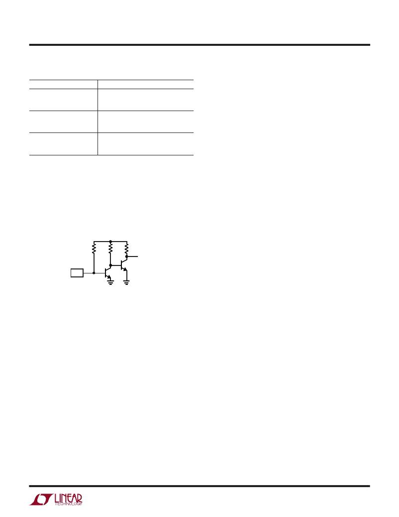
�The� circuit� shown� in� Figure� 7� provides� a� power� good�
�output� and� forces� continuous� operation.� Transistor� Q1�
�keeps� the� voltage� at� the� PGOOD� pin� below� 0.8V� thus�
�disabling� Burst� Mode� operation.� When� the� window� com-�
�parator� indicates� the� output� voltage� is� not� within� its� 7.5%�
�window,� the� base� of� Q1� is� pulled� to� ground� and� the� power�
�good� output� appearing� at� the� collector� of� Q2� goes� low.�
�INTV� CC�
�out� of� INTV� CC� that� is� typically� much� larger� than� the�
�control� circuit� current.� In� continuous� mode,� I� GATECHG� =�
�f(Q� T� +� Q� B� ),� where� Q� T� and� Q� B� are� the� gate� charges� of� the�
�topside� and� bottom-side� MOSFETs.�
�By� powering� EXTV� CC� from� an� output-derived� source� (or�
�other� high� efficiency� source),� the� additional� V� IN� current�
�resulting� from� the� driver� and� control� currents� will� be�
�scaled� by� a� factor� of� (Duty� Cycle)/(Efficiency).� For�
�example,� in� a� 15V� to� 1.8V� application,� 10mA� of� INTV� CC�
�current� results� in� approximately� 1.2mA� of� V� IN� current.�
�470k�
�100k�
�10k�
�This� reduces� the� midcurrent� loss� from� 10%� or� more� (if�
�PGOOD�
�PIN� 4�
�Q1�
�Q2�
�POWER�
�GOOD�
�the� driver� was� powered� directly� from� V� IN� )� to� only� a� few�
�percent.�
�3.� I� 2� R� losses� are� predicted� from� the� DC� resistances� of� the�
�1735-1� F07�
�Figure� 7.� Forced� Continuous� Operation� with� Power� Good� Indication�
�Efficiency� Considerations�
�The� percent� efficiency� of� a� switching� regulator� is� equal� to�
�the� output� power� divided� by� the� input� power� times� 100%.�
�It� is� often� useful� to� analyze� individual� losses� to� determine�
�what� is� limiting� the� efficiency� and� which� change� would�
�produce� the� most� improvement.� Percent� efficiency� can� be�
�expressed� as:�
�%Efficiency� =� 100%� –� (L1� +� L2� +� L3� +� ...)�
�where� L1,� L2,� etc.,� are� the� individual� losses� as� a� percent-�
�age� of� input� power.�
�Although� all� dissipative� elements� in� the� circuit� produce�
�losses,� four� main� sources� usually� account� for� most� of� the�
�losses� in� LTC1735-1� circuits:� 1)� LTC1735-1� V� IN� current,�
�2)� INTV� CC� current,� 3)� I� 2� R� losses,� 4)� Topside� MOSFET�
�transition� losses.�
�1.� The� V� IN� current� is� the� DC� supply� current� given� in� the�
�electrical� characteristics� which� excludes� MOSFET� driver�
�MOSFETs,� inductor� and� current� shunt.� In� continuous�
�mode,� the� average� output� current� flows� through� L� and�
�R� SENSE� ,� but� is� “chopped”� between� the� topside� main�
�MOSFET� and� the� synchronous� MOSFET.� If� the� two�
�MOSFETs� have� approximately� the� same� R� DS(ON)� ,� then�
�the� resistance� of� one� MOSFET� can� simply� be� summed�
�with� the� resistances� of� L� and� R� SENSE� to� obtain� I� 2� R�
�losses.� For� example,� if� each� R� DS(ON)� =� 0.02� ?� ,� R� L� =�
�0.03� ?� ,� and� R� SENSE� =� 0.01� ?� ,� then� the� total� resistance� is�
�0.06� ?� .� This� results� in� losses� ranging� from� 3%� to� 17%�
�as� the� output� current� increases� from� 1A� to� 5A� for� a� 1.8V�
�output,� or� 4%� to� 20%� for� a� 1.5V� output.� Efficiency�
�varies� as� the� inverse� square� of� V� OUT� for� the� same�
�external� components� and� power� level.� I� 2� R� losses� cause�
�the� efficiency� to� drop� at� high� output� currents.�
�4.� Transition� losses� apply� only� to� the� topside� MOSFET(s),�
�and� only� become� significant� when� operating� at� high�
�input� voltages� (typically� 12V� or� greater).� Transition�
�losses� can� be� estimated� from:�
�Transition� Loss� =� (1.7)� V� IN2� I� O(MAX)� C� RSS� f�
�19�
�相关PDF资料 |
PDF描述 |
|---|---|
| UPS2E470MHD | CAP ALUM 47UF 250V 20% RADIAL |
| RBC20DRYI-S734 | CONN EDGECARD 40POS DIP .100 SLD |
| UPM2E330MHD1TN | CAP ALUM 33UF 250V 20% RADIAL |
| VI-2WD-EW-F2 | CONVERTER MOD DC/DC 85V 100W |
| VI-JWN-EW-F4 | CONVERTER MOD DC/DC 18.5V 100W |
相关代理商/技术参数 |
参数描述 |
|---|---|
| LTC1735CGNPBF | 制造商:Linear Technology 功能描述:Regulator Synch Step Down LTC1735CGN |
| LTC1735CS | 功能描述:IC REG CTRLR BUCK PWM CM 16-SOIC RoHS:否 类别:集成电路 (IC) >> PMIC - 稳压器 - DC DC 切换控制器 系列:- 标准包装:2,500 系列:- PWM 型:电流模式 输出数:1 频率 - 最大:500kHz 占空比:96% 电源电压:4 V ~ 36 V 降压:无 升压:是 回扫:无 反相:无 倍增器:无 除法器:无 Cuk:无 隔离:无 工作温度:-40°C ~ 125°C 封装/外壳:24-WQFN 裸露焊盘 包装:带卷 (TR) |
| LTC1735CS#PBF | 功能描述:IC REG CTRLR BUCK PWM CM 16-SOIC RoHS:是 类别:集成电路 (IC) >> PMIC - 稳压器 - DC DC 切换控制器 系列:- 特色产品:LM3753/54 Scalable 2-Phase Synchronous Buck Controllers 标准包装:1 系列:PowerWise® PWM 型:电压模式 输出数:1 频率 - 最大:1MHz 占空比:81% 电源电压:4.5 V ~ 18 V 降压:是 升压:无 回扫:无 反相:无 倍增器:无 除法器:无 Cuk:无 隔离:无 工作温度:-5°C ~ 125°C 封装/外壳:32-WFQFN 裸露焊盘 包装:Digi-Reel® 产品目录页面:1303 (CN2011-ZH PDF) 其它名称:LM3754SQDKR |
| LTC1735CS#TR | 功能描述:IC REG CTRLR BUCK PWM CM 16-SOIC RoHS:否 类别:集成电路 (IC) >> PMIC - 稳压器 - DC DC 切换控制器 系列:- 标准包装:2,500 系列:- PWM 型:电流模式 输出数:1 频率 - 最大:500kHz 占空比:96% 电源电压:4 V ~ 36 V 降压:无 升压:是 回扫:无 反相:无 倍增器:无 除法器:无 Cuk:无 隔离:无 工作温度:-40°C ~ 125°C 封装/外壳:24-WQFN 裸露焊盘 包装:带卷 (TR) |
| LTC1735CS#TRPBF | 功能描述:IC REG CTRLR BUCK PWM CM 16-SOIC RoHS:是 类别:集成电路 (IC) >> PMIC - 稳压器 - DC DC 切换控制器 系列:- 标准包装:2,500 系列:- PWM 型:电流模式 输出数:1 频率 - 最大:500kHz 占空比:96% 电源电压:4 V ~ 36 V 降压:无 升压:是 回扫:无 反相:无 倍增器:无 除法器:无 Cuk:无 隔离:无 工作温度:-40°C ~ 125°C 封装/外壳:24-WQFN 裸露焊盘 包装:带卷 (TR) |
发布紧急采购,3分钟左右您将得到回复。