- 您现在的位置:买卖IC网 > PDF目录180126 > M306V8FJFP 16-BIT, FLASH, 16 MHz, MICROCONTROLLER, PQFP116 PDF资料下载
参数资料
| 型号: | M306V8FJFP |
| 元件分类: | 微控制器/微处理器 |
| 英文描述: | 16-BIT, FLASH, 16 MHz, MICROCONTROLLER, PQFP116 |
| 封装: | 20 X 20 MM, 0.65 MM PITCH, PLASTIC, LQFP-116 |
| 文件页数: | 43/77页 |
| 文件大小: | 2650K |
| 代理商: | M306V8FJFP |
第1页第2页第3页第4页第5页第6页第7页第8页第9页第10页第11页第12页第13页第14页第15页第16页第17页第18页第19页第20页第21页第22页第23页第24页第25页第26页第27页第28页第29页第30页第31页第32页第33页第34页第35页第36页第37页第38页第39页第40页第41页第42页当前第43页第44页第45页第46页第47页第48页第49页第50页第51页第52页第53页第54页第55页第56页第57页第58页第59页第60页第61页第62页第63页第64页第65页第66页第67页第68页第69页第70页第71页第72页第73页第74页第75页第76页第77页
M306V8FJFP
Rev.1.31
Apr 18, 2005
page 46 of 363
REJ03B0082-0131
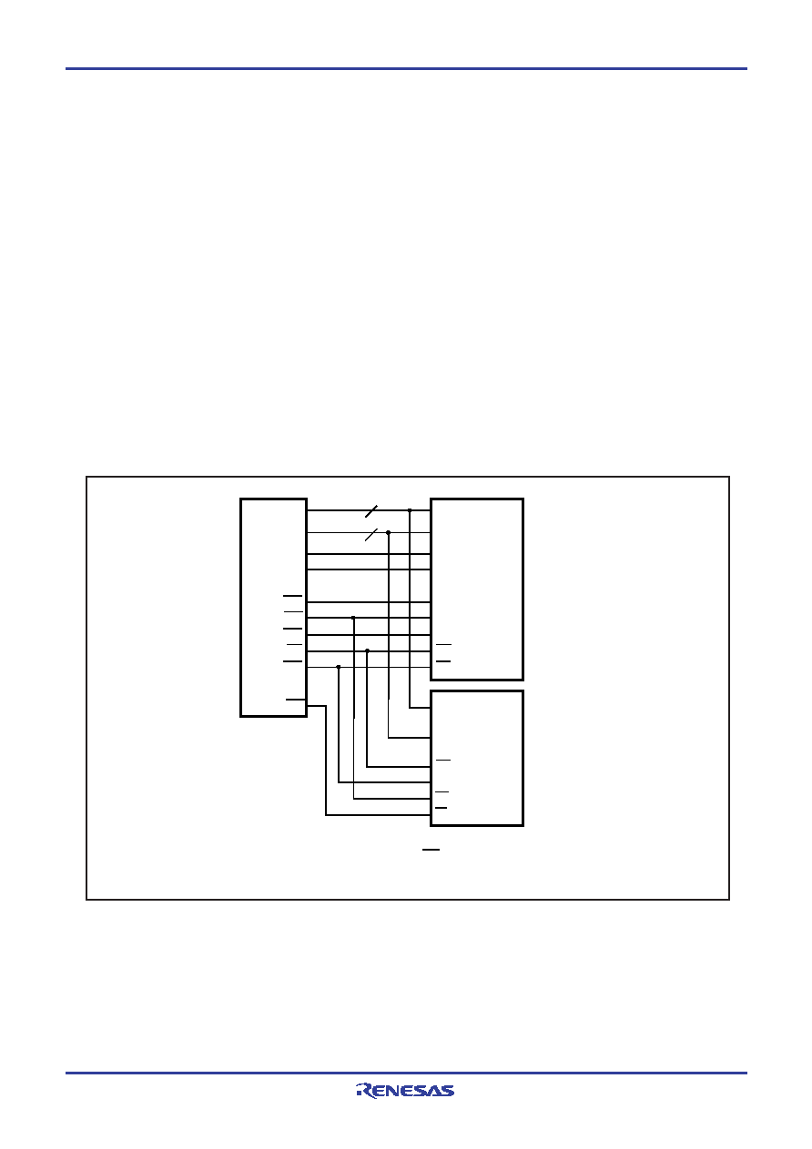
Figure 4.17 shows the external memory connect example in 4 Mbyte mode.
_____
_______
In this example, the CS pin of 4-Mbyte ROM is connected to the CS0 pin of microcomputer. The 4 Mbyte
_______
ROM address input AD21, AD20 and AD19 pins are connected to the CS3, CS2 and CS1 pins of micro-
computer, respectively. The address input AD18 pin is connected to the A19 pin of microcomputer. Fig-
ures 4.18 to 4.20 show the relationship of addresses between the 4-Mbyte ROM and the microcomputer
for the case of a connection example in Figure 4.17.
In microprocessor mode, or in memory expansion mode where the PM13 bit in the PM1 register is “0”,
banks are located every 512 Kbytes. Setting the OFS bit in the DBR register to “1”(offset) allows the
accessed address to be offset by 4000016, so that even the data overlapping a bank boundary can be
accessed in succession.
In memory expansion mode where the PM13 bit is “1”, each 512-Kbyte bank can be accessed in 256
Kbyte units by switching them over with the OFS bit.
____
_______
Because the SRAM can be accessed on condition that the chip select signals S2 = “H” and S1 =“L”, CS0
_______
____
and CS2 can be connected to S2 and S1, respectively. If the SRAM does not have the input pins to accept
____
_______
“H” active and “L” active chip select signals(S1, S2), CS0 and CS2 should be decoded external to the
chip.
17
8
M306V8
D0 to D7
A0 to A16
A17
RD
WR
CS1
CS2
CS3
CS0
A19
4M
bytes
ROM
DQ0 to DQ7
AD0 to AD16
AD17
AD18
AD19
OE
CS
128K
bytes
SRAM
DQ0 to DQ7
AD0 to AD16
S2
W
OE
S1
AD20
AD21
Note: If only one chip select pin (S1 or S2) is present,
decoding by use of an external circuit is required.
(Note)
Figure 4.17. External Memory Connect Example in 4M Byte Mode
相关PDF资料 |
PDF描述 |
|---|---|
| M30L40C-E3/4W | 15 A, 40 V, SILICON, RECTIFIER DIODE, TO-220AB |
| M31022AGLJFREQ | VCXO, CLOCK, 150 MHz - 1400 MHz, LVDS OUTPUT |
| M31002AMPJFREQ | VCXO, CLOCK, 150 MHz - 1400 MHz, PECL OUTPUT |
| M31022BGLNFREQ | VCXO, CLOCK, 150 MHz - 1400 MHz, LVDS OUTPUT |
| M31026ASLJFREQ | VCXO, CLOCK, 150 MHz - 1400 MHz, LVDS OUTPUT |
相关代理商/技术参数 |
参数描述 |
|---|---|
| M3-076 | 制造商:Southco 功能描述: |
| M3077 | 制造商:Tamura Corporation of America 功能描述: |
| M30800FCFP | 制造商:MITSUBISHI 制造商全称:Mitsubishi Electric Semiconductor 功能描述:SINGLE-CHIP 16-BIT CMOS MICROCOMPUTER |
| M30800FCFP#U3 | 功能描述:MCU 3/5V 128K I-TEMP PB-FREE 100 RoHS:是 类别:集成电路 (IC) >> 嵌入式 - 微控制器, 系列:M16C™ M16C/80 标准包装:160 系列:S08 核心处理器:S08 芯体尺寸:8-位 速度:40MHz 连通性:I²C,LIN,SCI,SPI 外围设备:LCD,LVD,POR,PWM,WDT 输入/输出数:53 程序存储器容量:32KB(32K x 8) 程序存储器类型:闪存 EEPROM 大小:- RAM 容量:1.9K x 8 电压 - 电源 (Vcc/Vdd):2.7 V ~ 5.5 V 数据转换器:A/D 12x12b 振荡器型:内部 工作温度:-40°C ~ 105°C 封装/外壳:64-LQFP 包装:托盘 |
| M30800FCGP | 制造商:MITSUBISHI 制造商全称:Mitsubishi Electric Semiconductor 功能描述:SINGLE-CHIP 16-BIT CMOS MICROCOMPUTER |
发布紧急采购,3分钟左右您将得到回复。