- 您现在的位置:买卖IC网 > PDF目录80583 > M38D59GF-XXXFP 8-BIT, MROM, 6.25 MHz, MICROCONTROLLER, PQFP80 PDF资料下载
参数资料
| 型号: | M38D59GF-XXXFP |
| 元件分类: | 微控制器/微处理器 |
| 英文描述: | 8-BIT, MROM, 6.25 MHz, MICROCONTROLLER, PQFP80 |
| 封装: | 14 X 20 MM, 0.80 MM PITCH, PLASTIC, QFP-80 |
| 文件页数: | 37/142页 |
| 文件大小: | 2004K |
| 代理商: | M38D59GF-XXXFP |
第1页第2页第3页第4页第5页第6页第7页第8页第9页第10页第11页第12页第13页第14页第15页第16页第17页第18页第19页第20页第21页第22页第23页第24页第25页第26页第27页第28页第29页第30页第31页第32页第33页第34页第35页第36页当前第37页第38页第39页第40页第41页第42页第43页第44页第45页第46页第47页第48页第49页第50页第51页第52页第53页第54页第55页第56页第57页第58页第59页第60页第61页第62页第63页第64页第65页第66页第67页第68页第69页第70页第71页第72页第73页第74页第75页第76页第77页第78页第79页第80页第81页第82页第83页第84页第85页第86页第87页第88页第89页第90页第91页第92页第93页第94页第95页第96页第97页第98页第99页第100页第101页第102页第103页第104页第105页第106页第107页第108页第109页第110页第111页第112页第113页第114页第115页第116页第117页第118页第119页第120页第121页第122页第123页第124页第125页第126页第127页第128页第129页第130页第131页第132页第133页第134页第135页第136页第137页第138页第139页第140页第141页第142页
Rev.3.04
May 20, 2008
Page 131 of 134
REJ03B0158-0304
38D5 Group
3. Executing STP Instruction
Executing the STP instruction sets the LCD enable bit (bit 4 of
LCD mode register1 (address 001316)) to “0” and the LCD panel
turns off. To turn the LCD panel on after returning from stop
mode, set the LCD enable bit to “1”.
4. VL3 Pin
To use the LCD drive control circuit while VL3 is set to the
voltage equal to VCC, apply the VCC voltage to the VL3 pin and
write “1” to the VL3 connection bit (bit 1 of LCD mode register 2
(address 001416)).
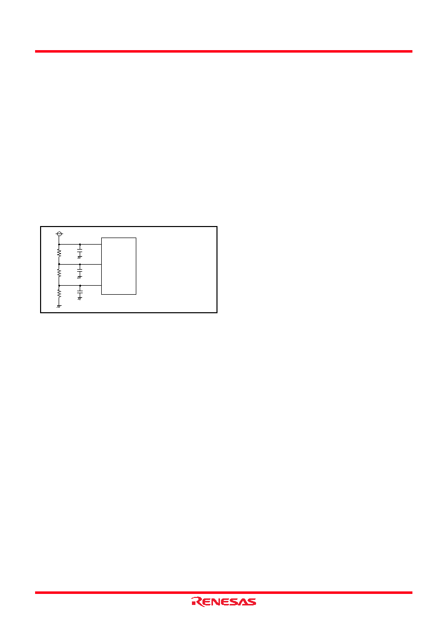
5. LCD Drive Power Supply
Fig. 106 Strengthening measure example of LCD drive
power supply
Notes on ROM Correction Function
1. Returning to Main Program
To return to the main program from the correction program, use
the JMP instruction (3-byte instruction).
2. Using ROM Correction Function
If the ROM correction function is used, be sure to enable the
ROM correction enable bit after setting the ROM correction
register.
3. Address
Do not set addresses other than the ROM area in the ROM
correction address registers. Also, do not set the same address in
the ROM correction address 1 register and the ROM correction
address 2 register.
4. ROM Correction Process
Include the ROM correction process in the program beforehand.
5. Using No ROM Correction Function
If the ROM correction function is not used, the ROM correction
vector can be used as normal RAM/ROM. When using as normal
RAM/ROM, be sure to set bits 1 and 0 of the ROM correction
enable register to “0” (disabled).
Notes on Clock Generating Circuit
1. Oscillation Circuit Constants
The oscillation circuit constants vary depending on the resonator.
Use values recommended by the oscillator manufacturer.
A feed-back resistor is implemented between the XIN and XOUT
pins (an external feed-back resistor may be required depending
on conditions). As no feed-back resistor is implemented between
XCIN and XCOUT, add a feedback resistor of about 10 M
.
2. Transition between Modes
When the MCU transits between on-chip oscillator mode, XIN
mode, or low-speed mode, both the XIN and XCIN oscillations
must be stabilized. Be especially careful when turning the power
on and returning from stop mode. Refer to the clock state
transition diagram for a transition between each mode. Also, set
the frequency in the condition that f(XIN)
≥ 3 × (XCIN).
When XIN mode is not used (the XIN-XOUT oscillation or
external clock input to XIN is not performed), connect XIN to
VCC through a resistor.
3. Oscillation Stabilization
Before executing the STP instruction, set the values * to generate
the wait time required for oscillation stabilization to timer 1 latch
and timer 2 latch (low-order 8 bits of timer 1 and high-order 8
bits of timer 2).
*Referential values
(Set values according to your oscillator and system)
OSCSEL = “L” in the flash memory and QzROM versions:
..................................................................... 000516 or more
OSCSEL = “H” in the QzROM version:
.....................................................................01FF16 or more
4. Low-Speed Mode, XIN Mode
To use low-speed mode or XIN mode, wait until oscillation
stabilizes after enabling the XIN-XOUT and XCIN-XCOUT
oscillation, then switch to the mode.
Connect by the shortest
possible wiring.
Connect the bypass capacitor
to the VL1
VL3 pins as short
as possible.
(Referential value:0.1
0.33 F)
VL3
VL2
VL1
相关PDF资料 |
PDF描述 |
|---|---|
| MC6805S3P | 8-BIT, MROM, MICROCONTROLLER, PDIP28 |
| MC908QT1AVDWE | 8-BIT, FLASH, 8 MHz, MICROCONTROLLER, PDSO8 |
| MC908QY4AVDT | 8-BIT, FLASH, 8 MHz, MICROCONTROLLER, PDSO16 |
| MC9S08AW16CFUE | 8-BIT, FLASH, 40 MHz, MICROCONTROLLER, PQFP64 |
| M902-01-156.2500LF | 156.25 MHz, OTHER CLOCK GENERATOR, CQCC36 |
相关代理商/技术参数 |
参数描述 |
|---|---|
| M38D59T-RLFS | 功能描述:BOARD EMULATOR FOR 38D5 GROUP RoHS:否 类别:编程器,开发系统 >> 内电路编程器、仿真器以及调试器 系列:- 产品变化通告:Development Systems Discontinuation 19/Jul/2010 标准包装:1 系列:* 类型:* 适用于相关产品:* 所含物品:* |
| M38DC-15 | 制造商:M/A-COM Technology Solutions 功能描述:MIXER(SPEC UX1015) - Bulk |
| M38K00F1-16FP | 制造商:MITSUBISHI 制造商全称:Mitsubishi Electric Semiconductor 功能描述:SINGLE-CHIP 8-BIT CMOS MICROCOMPUTER |
| M38K00F1-16HP | 制造商:MITSUBISHI 制造商全称:Mitsubishi Electric Semiconductor 功能描述:SINGLE-CHIP 8-BIT CMOS MICROCOMPUTER |
| M38K00F1-32FP | 制造商:MITSUBISHI 制造商全称:Mitsubishi Electric Semiconductor 功能描述:SINGLE-CHIP 8-BIT CMOS MICROCOMPUTER |
发布紧急采购,3分钟左右您将得到回复。