- 您现在的位置:买卖IC网 > PDF目录69017 > M66592WG UNIVERSAL SERIAL BUS CONTROLLER, PBGA64 PDF资料下载
参数资料
| 型号: | M66592WG |
| 元件分类: | 总线控制器 |
| 英文描述: | UNIVERSAL SERIAL BUS CONTROLLER, PBGA64 |
| 封装: | 0.80 MM PITCH, FBGA-64 |
| 文件页数: | 20/40页 |
| 文件大小: | 1583K |
| 代理商: | M66592WG |
第1页第2页第3页第4页第5页第6页第7页第8页第9页第10页第11页第12页第13页第14页第15页第16页第17页第18页第19页当前第20页第21页第22页第23页第24页第25页第26页第27页第28页第29页第30页第31页第32页第33页第34页第35页第36页第37页第38页第39页第40页
M66592F P/W G
Rev 1.00 2004.10.01 page 27 of 125
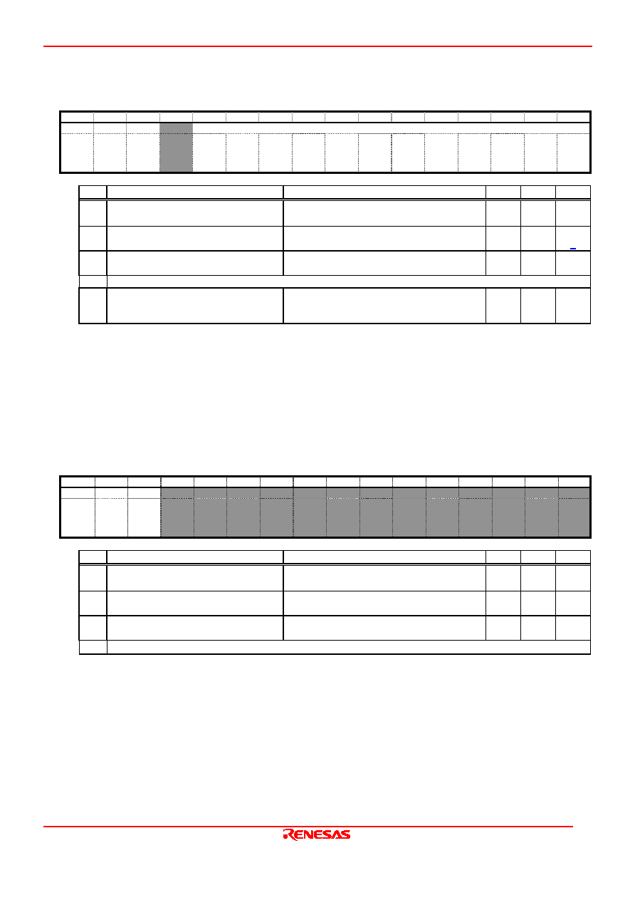
CFIFO port control register [CFIFOCTR]
<Address: 20H>
D0FIFO port control register [D0FIFOCTR]
<Address: 26H>
D1FIFO port control register [D1FIFOCTR]
<Address: 2CH>
15
14
13
12
11
10
9
8
7
6
5
4
3
2
1
0
BVAL
BCLR
FRDY
DTLN
0
-
0
-
0
-
0
?
0
-
0
-
0
-
0
-
0
-
0
-
0
-
0
-
0
-
0
-
0
-
0
-
0
Bit
Name
Function
S/W
H/W
Note
15 BVAL
Buffer Memory Valid flag
0: Invalid
1: Writing ended
R/ W(1) R/W
3.4.2
*6)
14 BCLR
CPU Buffer Clear
0: Invalid
1: Clears the buffer memory on the CPU side.
R(0)/
W(1)
R/W(0)
3.4
*7), *8)
13 FRDY
FIFO Port Ready
0: FIFO port access is disabled.
1: The FIFO port can be accessed.
R
W
3.4
*9)
12 Nothing is placed here. This should be fixed at “0”.
11-0 DTLN
Reception Data Length
The length of the reception data can be
confirmed.
R
W
3.4.2
3.4.4
*7)
Notes
*6) Writing “1” to the BVAL bit is valid when the direction of the data packet is the sending direction (when data is
being written to the buffer memory). When the direction is the receiving direction, “BVAL=0” should be set.
*7) The BCLR bit and DTLN bit are valid for the buffer memory on the CPU side. Software should set “BCLR=1” or
refer DTLN bit after making sure that “FRDY=1”.
*8) Using the BCLR bit to clear the buffer should be done with the pipe invalid state by the pipe configuration
(“PID=NAK”). When DCP is selected, the BCLR bit has the same function as the ACLRM bit of the PIPExCTR
register.
*9) The FRDY bit requires an access cycle of at least 450 ns after the pipe has been selected.
CFIFO port SIE register [CFIFOSIE]
<Address: 22H>
15
14
13
12
11
10
9
8
7
6
5
4
3
2
1
0
TGL
SCLR SBUSY
0
-
0
-
0
-
0
?
Bit
Name
Function
S/W
H/W
Note
15 TGL
Access Right Switch
0: Invalid
1: Switches access right
R(0)/
W(1)
R/W(0)
3.4.2
*10)
14 SCLR
SIE Buffer Clear
0: Invalid
1: Clears buffer memory on SIE side
R(0)/
W(1)
R/W(0)
3.4
*11)
13 SBUSY
SIE Buffer Busy
0: SIE is not being accessed.
1: SIE is being accessed.
R
W
3.4.2
12-0 Nothing is placed here. These should be fixed at “0”.
Note
*10) The function of the TGL bit is to set the buffer memory on the SIE side to the CPU side. Set “PID=NAK” and
check the SBUSY bit to make sure the SIE is not accessing the buffer (“SBUSY=0”). Then write the TGL bit
(toggle operation). This bit is valid only for pipes for which the reception direction (reading from the buffer
memory) has been set.
*11) The function of the SCLR bit is to clear the buffer memory on the SIE side. Set “PID=NAK” and check the
SBUSY
bit to make sure the SIE is not accessing the buffer (“SBUSY=0”). Then clear the buffer. This bit is valid
only for pipes for which the sending direction (writing to the buffer memory) has been set.
相关PDF资料 |
PDF描述 |
|---|---|
| M66596FP | UNIVERSAL SERIAL BUS CONTROLLER, PQFP64 |
| M68HC11D3CFB1 | 8-BIT, MROM, 1 MHz, MICROCONTROLLER, PQFP44 |
| M68HC711D0CFN | 8-BIT, 2 MHz, MICROCONTROLLER, PQCC44 |
| M68HC711D0CFB | 8-BIT, 2 MHz, MICROCONTROLLER, PQFP44 |
| M68HC711D3CFB1 | 8-BIT, MROM, 1 MHz, MICROCONTROLLER, PQFP44 |
相关代理商/技术参数 |
参数描述 |
|---|---|
| M66592WG#RB0Z | 制造商:Renesas Electronics Corporation 功能描述:USB 2 Peripheral Controller 64-Pin FBGA 制造商:Renesas 功能描述:USB 2 Peripheral Controller 64-Pin FBGA |
| M66596FP | 制造商:Renesas Electronics Corporation 功能描述:USB CONTROLLERS |
| M66596FP#RB0Z | 制造商:Renesas Electronics Corporation 功能描述:MCU - Trays 制造商:Renesas Electronics 功能描述:USB Device Controller 64-Pin LQFP Cut Tape 制造商:Renesas Electronics 功能描述:USB Device Controller 64-Pin LQFP Tray 制造商:Renesas 功能描述:USB Device Controller 64-Pin LQFP |
| M66596FPRB0Z | 制造商:Renesas Electronics Corporation 功能描述:USB2.0 Dual Function Controller,LQFP64 |
| M66596WG | 制造商:RENESAS 制造商全称:Renesas Technology Corp 功能描述:ASSP (USB2.0 Dual Function Controller) |
发布紧急采购,3分钟左右您将得到回复。