- 您现在的位置:买卖IC网 > PDF目录69017 > M66592WG UNIVERSAL SERIAL BUS CONTROLLER, PBGA64 PDF资料下载
参数资料
| 型号: | M66592WG |
| 元件分类: | 总线控制器 |
| 英文描述: | UNIVERSAL SERIAL BUS CONTROLLER, PBGA64 |
| 封装: | 0.80 MM PITCH, FBGA-64 |
| 文件页数: | 37/40页 |
| 文件大小: | 1583K |
| 代理商: | M66592WG |
第1页第2页第3页第4页第5页第6页第7页第8页第9页第10页第11页第12页第13页第14页第15页第16页第17页第18页第19页第20页第21页第22页第23页第24页第25页第26页第27页第28页第29页第30页第31页第32页第33页第34页第35页第36页当前第37页第38页第39页第40页
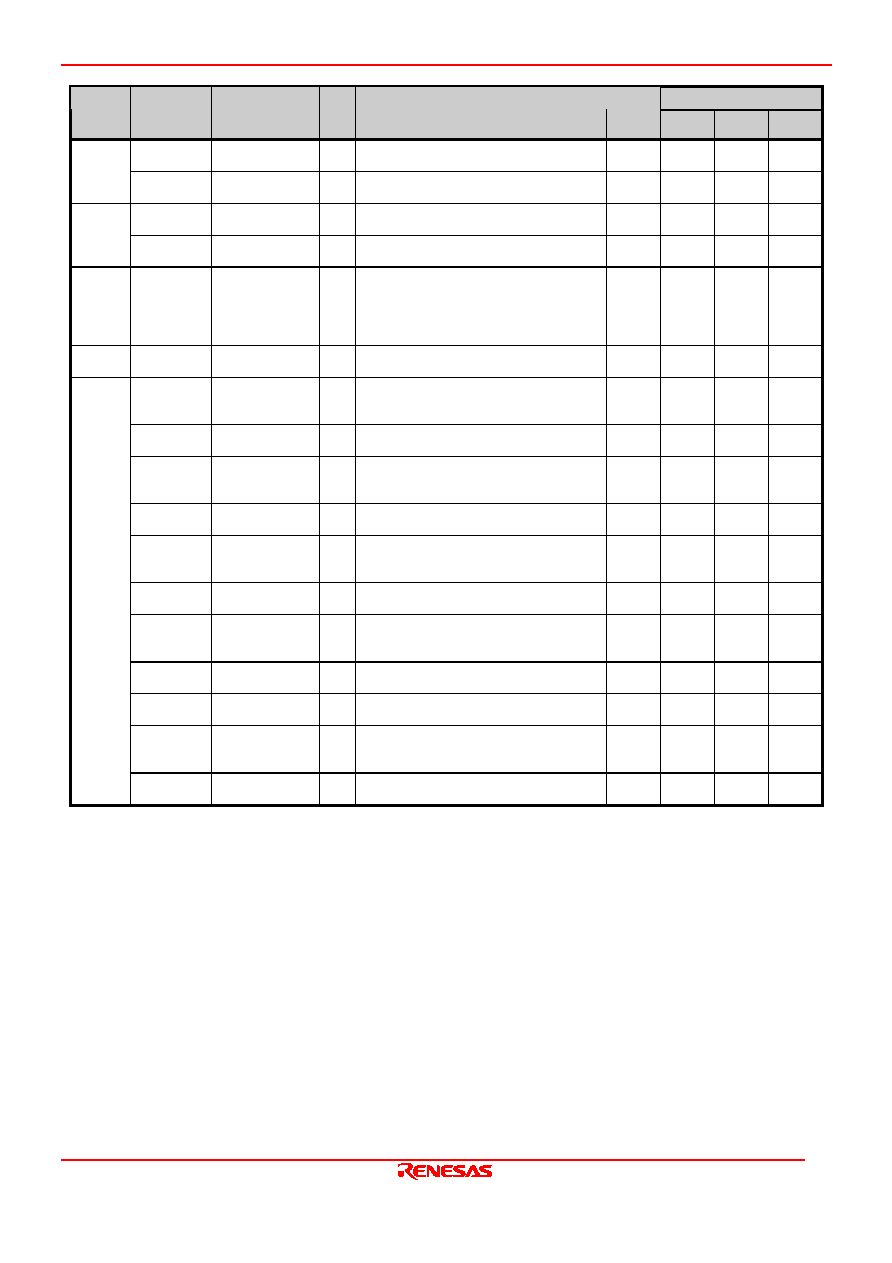
M66592F P/W G
Rev 1.00 2004.10.01 page 6 of 125
State of pin *7)
Category Pin name
Name
I/O
Function
Pin
count
(Pin nos.)
RST_N=”
L”
RST_N
goes “H”
PCUT=1
RST_N
Reset signal
IN
At “L” level, the controller is initialized.
1
(63)
Input
(L)
Input
(H)
Input
(H)
System
control
TEST
Test signal
IN
This should be fixed at “L” or open.
1
(16)
DP
USB D+ data
I/O
This should be connected to the D+ pin of
the USB bus.
1
(4)
Input
(Hi-z)
Input
(Hi-z)
Input
(Hi-z)
USB bus
interface
DM
USB D- data
I/O
This should be connected to the D- pin of
the USB bus.
1
(3)
Input
(Hi-z)
Input
(Hi-z)
Input
(Hi-z)
VBUS
monitor
input
VBUS
VBUS input
IN
This should be connected directly to the
Vbus of the USB bus. The connected or
disconnected state of the Vbus can be
detected. If This pin is not connectted with
Vbus of a USB bus, connect it with 5V.
1
(5)
Input
(Hi-z)
Input
(Hi-z)
Input
(Hi-z)
Reference
resistance
REFRIN
Reference input IN
This should be connected to AFEA33G
through a 5.6 k±1% resistance.
1
(8)
AFEA33V
Transceiver unit
analog power
supply
-
This should be connected to 3.3 V.
1
(12)
AFEA33G
Transceiver unit
analog GND
-
1
(9)
AFED33V
Transceiver unit
digital power
supply
-
This should be connected to 3.3 V.
1
(2)
AFED33G
Transceiver unit
digital GND
-
1
(1)
AFEA15V
Transceiver unit
analog 1.5 V
power supply
-
This should be connected to 1.5 V.
1
(6)
AFEA15G
Transceiver unit
analog GND
-
1
(7)
AFED15V
Transceiver unit
digital 1.5 V
power supply
-
This should be connected to 1.5 V.
1
(13)
AFED15G
Transceiver unit
digital GND
-
1
(14)
VDD
Core power
supply
-
This should be connected to 1.5 V.
1
(40)
VIF
IO power supply -
This should be connected to 3.3 V or 1.8
V.
3
(15, 42,
64)
Power
supply /
GND
DGND
Digital GND
-
1
(41)
*1) The “L” active and “H” active states of these pins can be specified using the control program for the user system.
”_N” indicates that the “L” active state is the default state.
*2) DSTB0_N and DACK1_N are assigned to the same pin, so the functions of one or the other are valid.
*3) The input level of the MPBUS pin needs to be established just before the end of H/W reset. Also, this should not
be switched during operation.
*4) When CS_N and RD_N are “L”, these pins output “H” or “L”.
*5) If MPBUS is “H”, these pins can be made to open.
*6) CS_N, WR0_N, and WR1_N should be kept as (a) or (b) during RST_N=”L” (from RST_N goes "L" to right after
RST_N goes "H").
(a) CS_N=”H”
(b) WR0_N=”H” and WR1_N=”H”
*7) Discription of “State of pin”
(a) Input : Pins are Hi-z state. Please do not make it “open” on a board.
(b) Input(Hi-z) : Pins are Hi-z state. Pins can be “open” on a board.
(c) H, L, H/L : Output states is shown.
*8) These pins are in an inactive state.
相关PDF资料 |
PDF描述 |
|---|---|
| M66596FP | UNIVERSAL SERIAL BUS CONTROLLER, PQFP64 |
| M68HC11D3CFB1 | 8-BIT, MROM, 1 MHz, MICROCONTROLLER, PQFP44 |
| M68HC711D0CFN | 8-BIT, 2 MHz, MICROCONTROLLER, PQCC44 |
| M68HC711D0CFB | 8-BIT, 2 MHz, MICROCONTROLLER, PQFP44 |
| M68HC711D3CFB1 | 8-BIT, MROM, 1 MHz, MICROCONTROLLER, PQFP44 |
相关代理商/技术参数 |
参数描述 |
|---|---|
| M66592WG#RB0Z | 制造商:Renesas Electronics Corporation 功能描述:USB 2 Peripheral Controller 64-Pin FBGA 制造商:Renesas 功能描述:USB 2 Peripheral Controller 64-Pin FBGA |
| M66596FP | 制造商:Renesas Electronics Corporation 功能描述:USB CONTROLLERS |
| M66596FP#RB0Z | 制造商:Renesas Electronics Corporation 功能描述:MCU - Trays 制造商:Renesas Electronics 功能描述:USB Device Controller 64-Pin LQFP Cut Tape 制造商:Renesas Electronics 功能描述:USB Device Controller 64-Pin LQFP Tray 制造商:Renesas 功能描述:USB Device Controller 64-Pin LQFP |
| M66596FPRB0Z | 制造商:Renesas Electronics Corporation 功能描述:USB2.0 Dual Function Controller,LQFP64 |
| M66596WG | 制造商:RENESAS 制造商全称:Renesas Technology Corp 功能描述:ASSP (USB2.0 Dual Function Controller) |
发布紧急采购,3分钟左右您将得到回复。