- 您现在的位置:买卖IC网 > PDF目录18820 > MAX11008BETM+ (Maxim Integrated)IC CTLR LDMOS BIAS DUAL 48TQFN PDF资料下载
参数资料
| 型号: | MAX11008BETM+ |
| 厂商: | Maxim Integrated |
| 文件页数: | 13/67页 |
| 文件大小: | 0K |
| 描述: | IC CTLR LDMOS BIAS DUAL 48TQFN |
| 产品培训模块: | Lead (SnPb) Finish for COTS Obsolescence Mitigation Program |
| 标准包装: | 43 |
| 功能: | 偏压控制器 |
| RF 型: | 手机 |
| 次要属性: | 片上 4Kb EEPROM |
| 封装/外壳: | 48-WFQFN 裸露焊盘 |
| 包装: | 托盘 |
第1页第2页第3页第4页第5页第6页第7页第8页第9页第10页第11页第12页当前第13页第14页第15页第16页第17页第18页第19页第20页第21页第22页第23页第24页第25页第26页第27页第28页第29页第30页第31页第32页第33页第34页第35页第36页第37页第38页第39页第40页第41页第42页第43页第44页第45页第46页第47页第48页第49页第50页第51页第52页第53页第54页第55页第56页第57页第58页第59页第60页第61页第62页第63页第64页第65页第66页第67页
�� �
�
�Dual� RF� LDMOS� Bias� Controller� with�
�Nonvolatile� Memory�
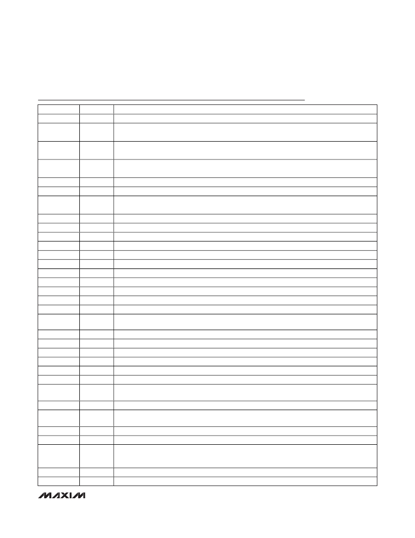
�Pin� Description�
�PIN�
�1,� 31�
�2�
�3�
�4�
�5�
�6�
�7�
�8�
�9�
�10�
�11�
�12�
�13�
�14�
�15�
�16�
�17�
�18�
�19,� 25,� 30,�
�34–39,� 42,� 48�
�20,� 24�
�21,� 22,� 23�
�26�
�27�
�28�
�29�
�32,� 33,� 47�
�40�
�41�
�43�
�44�
�45�
�46�
�—�
�NAME�
�DGND�
�OPSAFE1�
�A0/� CS�
�CNVST�
�SPI/� I2C�
�ALARM�
�OPSAFE2�
�REFDAC�
�REFADC�
�DXP1�
�DXN1�
�DXP2�
�DXN2�
�ADCIN1�
�ADCIN2�
�PGAOUT2�
�GATE2�
�GATE1�
�N.C.�
�AV� DD�
�AGND�
�CS2+�
�CS2-�
�CS1-�
�CS1+�
�DV� DD�
�PGAOUT1�
�A2/N.C.�
�SCL/SCLK�
�SDA/DIN�
�A1/DOUT�
�BUSY�
�EP�
�FUNCTION�
�Digital� Ground.� Connect� both� DGND� inputs� to� the� same� potential.�
�Output� Safe� Switch� Logic� Input� 1.� Drive� OPSAFE1� high� to� close� the� output� safe� switch� and� clamp�
�GATE1� to� AGND.� Drive� OPSAFE1� low� to� open� the� switch.�
�Address-Select� Input� 0/Chip-Select� Input.� In� I� 2� C� mode,� this� is� the� address-select� input� 0.� See� Table�
�1.� In� SPI� mode,� this� is� the� chip-select� input.�
�Active-Low� Conversion� Start� Input.� Drive� CNVST� low� to� begin� a� conversion� when� in� clock� modes� 01�
�and� 11.�
�Interface-Select� Input.� Connect� to� DGND� for� I� 2� C� interface.� Connect� to� DV� DD� for� SPI� interface.�
�Alarm� Output�
�Output� Safe� Switch� Logic� Input� 2.� Drive� OPSAFE2� high� to� close� the� output� safe� switch� and� clamp�
�GATE2� to� AGND.� Drive� OPSAFE2� low� to� open� the� switch.�
�DAC� Reference� Input/Output�
�ADC� Reference� Input/Output�
�Temperature� Diode� Positive� Input� 1.� Connect� DXP1� to� the� anode� of� the� external� diode.�
�Temperature� Diode� Negative� Input� 1.� Connect� DXN1� to� the� cathode� of� the� external� diode.�
�Temperature� Diode� Positive� Input� 2.� Connect� DXP2� to� the� anode� of� the� external� diode.�
�Temperature� Diode� Negative� Input� 2.� Connect� DXN2� to� the� cathode� of� the� external� diode.�
�ADC� Auxiliary� Input� 1�
�ADC� Auxiliary� Input� 2�
�Programmable-Gain� Amplifier� Output� 2�
�Gate-Drive� Amplifier� Output� 2�
�Gate-Drive� Amplifier� Output� 1�
�No� Connection.� Not� internally� connected.� Leave� unconnected.�
�Analog-Supply� Input.� Connect� both� AV� DD� inputs� to� the� same� potential.�
�Analog� Ground.� Connect� all� AGND� inputs� to� the� same� potential.�
�Current-Sense� Positive� Input� 2.� CS2+� is� the� external� sense-resistor� connection� to� the� LDMOS� 2� supply.�
�Current-Sense Negative Input 2. CS2- is the external sense-resistor connection to the LDMOS 2 drain.�
�Current-Sense Negative Input 1. CS1- is the external sense-resistor connection to the LDMOS 1 drain.�
�Current-Sense� Positive� Input� 1.� CS1+� is� the� external� sense-resistor� connection� to� the� LDMOS� 1� supply.�
�Digital-Supply� Input.� Connect� all� DV� DD� inputs� to� the� same� potential.� Connect� a� 0.1μF� capacitor� to�
�DV� DD� .�
�Programmable-Gain� Amplifier� Output� 1�
�Address-Select� Input� 2/N.C.� In� I� 2� C� mode,� this� pin� is� the� address-select� input� 2.� See� Table� 1.� In� SPI�
�mode,� this� is� a� no� connection� pin.�
�Serial-Clock� Input.� SCL� is� the� I� 2� C-compatible� clock� input.� SCLK� is� the� SPI-compatible� clock� input.�
�Serial-Data� Input/Output.� SDA� is� the� I� 2� C-compatible� input/output.� DIN� is� the� SPI-compatible� data� input.�
�Address-Select� Input� 1/Data� Out.� In� I� 2� C� mode,� this� is� the� address-select� input� 1.� See� Table� 1.� In� SPI�
�mode,� this� is� the� serial-data� output.� Data� is� clocked� out� on� the� falling� edge� of� SCLK.� DOUT� is� a� high-�
�impedance� output� when� CS� is� driven� high.�
�Busy� Output.� BUSY� goes� high� to� indicate� activity.�
�Exposed� Pad.� Connect� EP� to� AGND.� Internally� connected� to� AGND.�
�______________________________________________________________________________________�
�13�
�相关PDF资料 |
PDF描述 |
|---|---|
| MCD310-16IO1 | MOD THYRISTOR/DIODE 1600V Y2-DCB |
| AH173-WL-7-B | IC HALL SENSOR LATCH 25MA SC59-3 |
| ACH3218-151-TD01 | FILTER 3-TERM 240MHZ 1.5A SMD |
| ND431425 | SCR MOD ISO DUAL 1400V 250A |
| AH175-WL-7-B | IC HALL SENSOR LATCH 25MA SC59-3 |
相关代理商/技术参数 |
参数描述 |
|---|---|
| MAX11008BETM+ | 功能描述:射频放大器 Dual RF LDMOS Bias Controller w/NV Mem RoHS:否 制造商:Skyworks Solutions, Inc. 类型:Low Noise Amplifier 工作频率:2.3 GHz to 2.8 GHz P1dB:18.5 dBm 输出截获点:37.5 dBm 功率增益类型:32 dB 噪声系数:0.85 dB 工作电源电压:5 V 电源电流:125 mA 测试频率:2.6 GHz 最大工作温度:+ 85 C 安装风格:SMD/SMT 封装 / 箱体:QFN-16 封装:Reel |
| MAX11008BETM+T | 功能描述:射频放大器 Dual RF LDMOS Bias Controller w/NV Mem RoHS:否 制造商:Skyworks Solutions, Inc. 类型:Low Noise Amplifier 工作频率:2.3 GHz to 2.8 GHz P1dB:18.5 dBm 输出截获点:37.5 dBm 功率增益类型:32 dB 噪声系数:0.85 dB 工作电源电压:5 V 电源电流:125 mA 测试频率:2.6 GHz 最大工作温度:+ 85 C 安装风格:SMD/SMT 封装 / 箱体:QFN-16 封装:Reel |
| MAX11008EVC16 | 功能描述:放大器 IC 开发工具 MAX11008 Eval Kit RoHS:否 制造商:International Rectifier 产品:Demonstration Boards 类型:Power Amplifiers 工具用于评估:IR4302 工作电源电压:13 V to 23 V |
| MAX11008EVKIT+ | 功能描述:放大器 IC 开发工具 MAX11008 Eval Kit RoHS:否 制造商:International Rectifier 产品:Demonstration Boards 类型:Power Amplifiers 工具用于评估:IR4302 工作电源电压:13 V to 23 V |
| MAX1100CWG | 制造商:Rochester Electronics LLC 功能描述: 制造商:Maxim Integrated Products 功能描述: |
发布紧急采购,3分钟左右您将得到回复。